Department for Physics and Astronomy University of Heidelberg - Lukas Endres 2020 Master Thesis in Physics submitted by born in Bamberg (Germany) ...
←
→
Page content transcription
If your browser does not render page correctly, please read the page content below
Department for Physics and Astronomy
      University of Heidelberg

           Master Thesis in Physics
                submitted by

            Lukas Endres
          born in Bamberg (Germany)

                   2020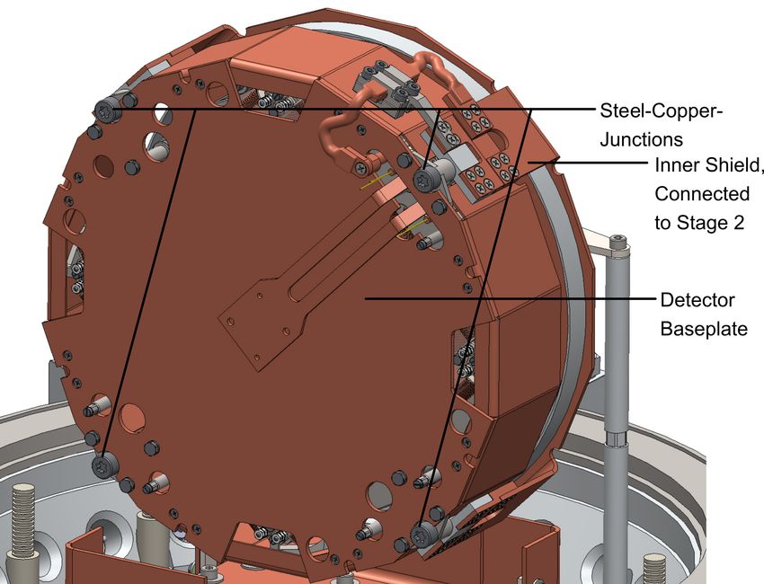
Cryogenic Characterization
of a Microchannel Plate Detector

 This Master Thesis was carried out by Lukas Endres
                        at the
Max Planck Institute for Nuclear Physics in Heidelberg
              under the supervision of
        Priv.-Doz. Dr. Robert Moshammer
                         and
              Prof. Dr. Thomas Pfeifer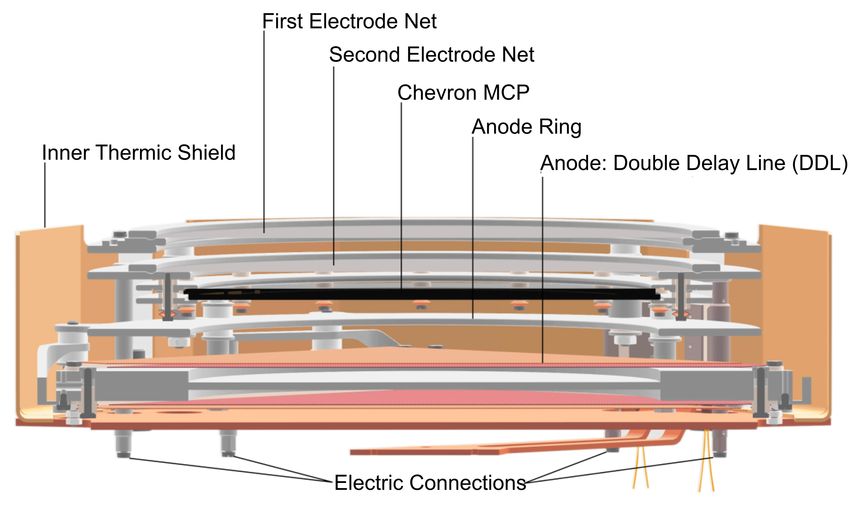
A cryogenic test setup for microchannel plate detectors was built
up and put into operation. Microchannel plates with a quality diameter
of 120 mm and an open area ratio of 0.6 are tested. During measurements
they can be cooled down to 35 K. A possibility to counteract the conse-
quences of thermal contraction of different construction parts with CuBe
cup springs was found. The thermal connection between the second stage
of a coldhead and the channel plates was optimized using a copper braid
and a suitable wiring of the detector. The final saturation and linearity
measurements show that the used channel plates are nearly unaffected
by a temperature change from room temperature to 35 K. Only the supply
voltage where the channel plates operate near the saturation region is
assumed to decrease slightly. The setup has to be further refined to enable
a lower temperature for channel plate tests.

Ein kryogener Teststand für Microchannel-Plate-Detektoren wurde
aufgebaut und in Betrieb genommen. Microchannel-Plates mit einem effek-
tiven Durchmesser von 120 mm und einem Open Area Ratio von 0.6 werden
getestet. Während der Messungen können diese bis zu einer Temperatur
von 35 K gekühlt werden. Es wurde eine Möglichkeit gefunden den Konse-
quenzen der thermischen Kontraktion verschiedener Konstruktionselemente
mit CuBe Tellerfedern entgegenzuwirken. Die thermische Ankopplung zwis-
chen der zweiten Stufe eines Kaltkopfes und den Channel-Plates wurde
optimiert, indem eine Kupfer-Litze hinzugefügt und eine geeignete Verka-
belung gefunden wurde. Die finalen Sättigungs- und Linearitätsmes-
sungen ergaben, dass die Channel-Plates bei einer Temperaturänderung
von Raumtemperatur zu 35 K nahezu unbeeinflusst bleiben. Lediglich
die Versorgungsspannung, bei der die Channel-Plates nahe der Sättigung
betrieben werden, sank geringfügig. Der Aufbau muss dahingehend weiter-
entwickelt werden, dass die Channel-Plates bei niedrigeren Temperaturen
getestet werden können.
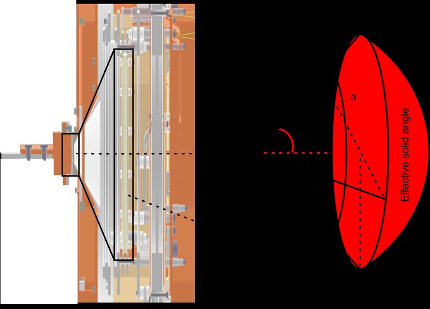
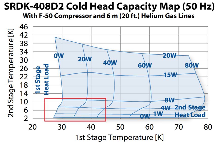
Table of Contents
1. Motivation                                                                       1

2. Relevant Considerations of Condensed Matter Physics                               3
   2.1. Electrical Conductivity . . . . . . . . . . . . . . .   .   .   .   .   .    3
        2.1.1. Electrical Transport in Metals . . . . . . .     .   .   .   .   .    3
        2.1.2. Electrical Transport in Semiconductors . .       .   .   .   .   .    6
        2.1.3. Electrical Transport in Amorphous Solids .       .   .   .   .   .    7
        2.1.4. Electrical Transport in MCPs . . . . . . .       .   .   .   .   .   10
   2.2. Linear Thermal Contraction . . . . . . . . . . . .      .   .   .   .   .   10

3. Microchannel Plate Detectors                                                     13
   3.1. Basic Parameters of MCPs . . . . . . . . . . . . . . . . . .                13
        3.1.1. Saturation Properties . . . . . . . . . . . . . . . . .              15
        3.1.2. Pulse Height Distribution . . . . . . . . . . . . . .                17
        3.1.3. Efficiency and Dead Time . . . . . . . . . . . . . .                 17
   3.2. MCP Detector Construction . . . . . . . . . . . . . . . . .                 20
        3.2.1. Cup Springs Counteracting the Consequence of Ther-
               mal Contraction . . . . . . . . . . . . . . . . . . . .              21
        3.2.2. Voltage Supply . . . . . . . . . . . . . . . . . . . .               23
   3.3. Readout Technique and Data Acquisition . . . . . . . . . .                  25

4. Experimental Setup                                                               28
   4.1. List of Used Devices . . . . . . . . . . . . . . . . . . . . .              32
   4.2. Alpha Source and Effective Solid Angle . . . . . . . . . . .                33
   4.3. Thermal Connection towards the MCP . . . . . . . . . . .                    34

5. Detector Characterization                                                        40
   5.1. Saturation Properties . . . . . . . . . . . . . . . . . . . . .             42
   5.2. Detector Linearity . . . . . . . . . . . . . . . . . . . . . .              45

                                     vii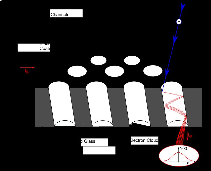
viii                                                      Table of Contents

6. Discussion and Outlook                                                   48
   6.1. Results . . . . . . . . . . . . . . . . . . . . . . . . . . . . .   48
   6.2. Possible Future Improvements . . . . . . . . . . . . . . . .        49

A. Appendix                                                                   i

Bibliography                                                                iii
1. Motivation
         My goal is simple. It is a complete understanding of the
              universe, why it is as it is and why it exists at all.
                                                      Hawking [1]
         Occurrences in this domain are beyond the reach of exact
       prediction because of the variety of factors in operation, not
               because of any lack of order in nature.a Einstein [2]
        a
            Although Einstein referred to the complexity of weather predictions,
             the statement can be transferred to a multitude of experimental
             measurements.

Stephen Hawking and Albert Einstein, two of the most famous thinkers
of late modern times, comitted their lifes to physical insights. After the
discovery of general relativity by Einstein in the early 20th century, Hawk-
ing focused on the theory of black holes and cosmological coherences. The
problem with such theories is that they are typically far beyond the scope
of surrounding conditions present on earth, so they can not be easily tested.
Here the work of experimental physicists becomes important. Space observ-
ing imaging systems provided the first proofs for general relativity as the
effect of gravitational lensing was discovered and for the existence of black
holes by “simply” photographing one [3]. Spectroscopic methods taught us
about the composition of stars and the interstellar medium. Thus, another
interesting observation was made in the early 20th century. Eddington
reported on the origin of “interstellar chemistry” after the discovery of
spectral absorption lines in the spectrum of a star caused by the interstellar
medium [4]. Nowadays, it is known that the absorption takes place in in-
terstellar clouds, huge regions of cold matter of low densities in interstellar
space. More recent spectroscopic experiments show that diffuse clouds are
mainly monoatomic, while dense clouds also contain large and particularly
stable molecules; around 50% of them being unusual at terrestrial standards
[5]. Due to the lack of thermal energy, chemical reactions forming these

                                           1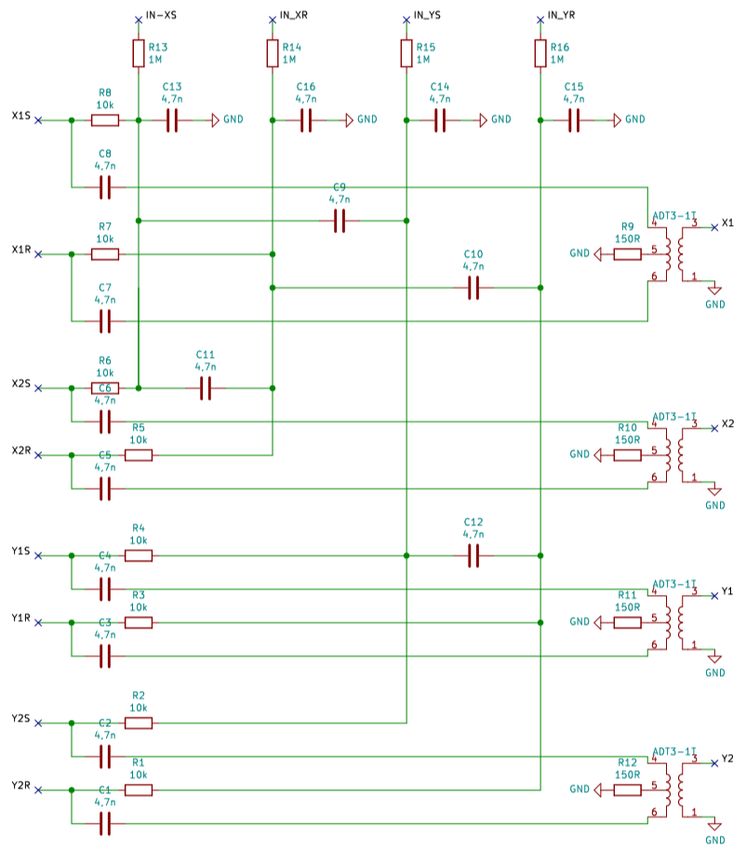
2                                                             1. Motivation

molecules are mainly triggered by collisions of the reactants themselves or of
reactants with cosmic rays. Theory provides rate coefficients for a multitude
of reactions but experimental confirmations are needed. Therefore (and
for other experiments using cold molecular ions), the Cryogenic Storage
Ring (CSR) was built at the Max Planck Institute for Nuclear Physics
in Heidelberg - first announced in Zajfman et al. [6]. A concept and its
technical realization were presented by von Hahn et al. [7]. The CSR is
capable of creating a few Kelvin environment with residual gas pressures of
down to a few 10−15 mbar, comparable to the interstellar medium. Injected
atomic or molecular ions are electrostatically guided onto a closed trajectory.
After the collision of the cold molecular ion beam with a supersonic gas
jet a kinematically complete analysis of the produced fragments will be
executed using a Reaction Microscope [8; 9; 10]. For particle detection
microchannel plate detectors are used, the core of this work.

   Due to the extreme environment inside the CSR, it has to be elaborated
if the microchannel plate detector can provide sufficient detection efficiency.
Especially for experiments where several fragments have to be detected
coincidently a high detection efficiency is needed. The lower the efficiency,
the longer acquiring significant statistics takes and the more expensive
the measurement becomes. Contrary to that, heating the detector for
higher efficiency should not have a significant effect on the costly produced
measurement environment inside the reaction microscope. It is already
known, that in general the efficiency decreases with temperature but for
exact predictions the specific microchannel plate in use has to be char-
acterized adequately. The main goal of this work is to characterize the
behavior of the used channel plate detector in a cryogenic environment.
A cryogenic test setup is built up and put into operation such that the
detector can be tested at temperatures between 35 K and room temperature.
The result of this work will contribute to the huge project CSR and its
successful measurements which will conduce to new insights in the field of
astrochemistry.
2. Relevant Considerations of
   Condensed Matter Physics
In this chapter a compact overview of the topics electrical conductivity and
thermal contraction is given. Since general properties of solids is a wide
ranged field we only focus on the aspects relevant for this thesis. More
information is given in typical condensed matter literature i.e. Hunklinger
[11], Chapter 3-10, and Gross Marx [12], Chapter 1,2 and 4-10. The
main goal is to achieve insights into the temperature dependent electrical
properties of amorphous semiconductors i.e. glasses, out of which Micro-
Channel Plates (MCPs) are made.

2.1. Electrical Conductivity
A large class of solids can be treated as a periodic structure where the
smallest repeating unit is called primitive cell. Those primitive cells are
essential for the properties of a solid, because they define the Brillouin
zones which contain all possible momentum vectors ~k describing lattice
oscillations in real space (= phonons). Since phonons play a bigger role in
the transport of thermal energy, the focus in the following analysis will be
layed on the energy band model for electrons inside a periodic potential.
Similar to the phonons, electrons can be fully described by restriction to
the first Brillouin zone. The potential landscape then reduces to the energy
band structure, see Hunklinger [11], Chapter 8.5 and Gross Marx [12],
Chapter 8.

2.1.1. Electrical Transport in Metals
If one wants to understand the processes relevant for the transport of
electrical charge inside a solid, one has to understand the interactions of

                                     3
4 2. Relevant Considerations of Condensed Matter Physics
conducting electrons with the solid itself. The clearest model is developed
for metals which have a full valence band and a partially filled conduction
band. The first proper model describing electrical conduction in metals
was presented by Drude. He used the classical picture of a free electron gas
which is a good assumption for electrons in the conduction band of metals,
with average drift velocity vd and relaxation time τ . Although he neglected
the Fermi-Dirac distribution and hence followed a wrong calculation, he
ended up with the correct solution for the electron mobility µ and the
conductivity σ:
eτ
µ= , (2.1)
me
ne2 τ
σ= = neµ, (2.2)
me
with the electron mass me , the electron density n and the elementary charge
e.
Figure 2.1.: Scheme of the displacement of the Fermi energy surface in momen-
tum space. The initial Fermi sphere EF is displaced by a constant electric field
until the equilibrium state EF∗ is reached. In this scheme the applied electric
field is oriented parallel to the spatial x-axis, hence the Fermi sphere moves in
x-direction.
A more advanced approach was later presented by Sommerfeld. He treated
the electrons as quasi-free fermions, following the Schrödinger equation and2.1. Electrical Conductivity 5
the Pauli principle. The model itself uses the Fermi surface of electrons
and its interaction with an external constant electrical field E.
~ The E-field
~
E = E~e pushes the Fermi surface in k-space EF (k) in ~e-direction, until a
~
dynamic equilibrium is reached where scattering processes between electrons
and e.g. phonons prohibit a further displacement of EF (~k) (see Figure 2.1).
Using the Boltzmann equation and the relaxation approach Sommerfeld
calculated for the conductivity σ of an isotropic gas of free electrons
e2 τ (EF ) 3 ne2
σ= k = τ (EF ), (2.3)
3π 2 m∗ F m∗
with the effective
√ electron mass m∗ , the electron density n and the wave
vector kF = 3π 2 n of those electrons with Fermi Energy EF . To reach this
3
result he also assumed that only electrons near the Fermi energy contribute
to the electrical charge transport. The essential part of Equation 2.3 is the
relaxation time τ which determines the time until the Fermi surface reaches
equilibrium after turning on the electrical field. τ is the result of different
scattering processes and therefore characteristic for different temperature
regions:
i) electron-electron scattering: (τe ),
ii) electron-phonon scattering: (τp ),
iii) electron-defect scattering: (τd ).
Since (i-iii) are independent scattering processes one can write
1 1 1 1
= + + . (2.4)
τ τe τp τd
For very clean metals with high purity and few vacancies mainly electron-
phonon scattering is present. At high temperatures (T > θ)1 the electrons
mainly scatter with phonons at Debye frequency. According to the inverse
mean free path l−1 = nph · σscat , using a constant cross section σscat for
electrons near EF and phonons of frequency ωDebye , the temperature depen-
dency in this region is characterized by the phonon density nph . At high
1
θ is the so called Debye temperature, a material dependent constant. It is linked to
the maximum frequency of phonos ωDebye present in a solid.6 2. Relevant Considerations of Condensed Matter Physics
temperatures T , it applies nph ∝ T which yields to l−1 ∝ T and finally
gives σ ∝ l ∝ T −1 .
With decreasing temperature the total number of phonons and their
frequency decreases. Here one has to apply the Bloch-Grüneisen law for
the resistivity ρ ∝ σ −1 which is valid for all metals where electron phonon
scattering is dominant:
x5 dx
5 Z θ/T
T
ρ=A . (2.5)
θ 0 (ex − 1)(1 − e−x )
Without going into detail one calculates:
T 5
T →0: ρ∝ , (2.6)
θ
T
T →θ: ρ∝ . (2.7)
θ
At temperatures near absolute zero (T < 10 K) phonons are negligible
and a constant number of lattice defects are left as scattering partners. In
total the temperature dependent resistivity of metals can be described as
following:
const : T
θ (only defects),
ρ∝ T 5 : T < θ, (2.8)
: T > θ.
T
The resistance of metals decreases with temperature until a constant value
which depends on the number of defects in the metal, is reached.
2.1.2. Electrical Transport in Semiconductors
The main difference between metals and semiconductors is the number of
occupied states in the conduction band. While the conduction band in met-
als is occupied by electrons independently of temperature, the conduction
band of semiconductors gets populated by thermally excited electrons which
are lifted from the valence band. The essential quantity is the band-gap2.1. Electrical Conductivity 7
energy Eg = Ec − Ev , with the minimum energy of the conduction band Ec
and the maximum energy of the valence band Ev . The band gap is typically
in the order of a few eV, for example silicon has a band gap of Eg = 1.1 eV.
Hence, a semiconductor behaves as an insulator at T = 0 K. This implies a
zero-crossing of the mobility at absolute zero. With increasing temperature
electrons start to occupy the conduction band and the semiconductor be-
comes electrically conductive.
One distinguishes between intrinsic and doped semiconductors. The
former ones have in common that the number of electrons in the conduction
band is always equal to the number of holes in the valence band. The
latter ones contain foreign atoms which dramatically influence the electrical
properties by delivering free electrons to the conduction band (donators) or
by extracting electrons out of the valence band (acceptors).
As shown in Section (2.1.1) the mobility of electrons and hence the electrical
conductivity of solids is mainly restricted by scattering processes. Again
the dominant process in a definite temperature region determines the
temperature dependent electrical conductivity. For small temperatures (T ≈
50 K) electron-impurity scattering is dominant while for higher temperatures
electron-phonon scattering is dominant. One finds:
T 3/2 : T < 50 K,
(
µ∝ (2.9)
T −3/2 : T > 50 K.
2.1.3. Electrical Transport in Amorphous Solids
In amorphous semiconductors one has to modify the relaxation and scatter-
ing approach, since the periodic structure used to analyze metals or regular
semiconductors is missing. The band structure of a crystal is formed by
the periodicity of atomic levels, this is restricted to a near field ordering in
amorphous solids. N.F. Mott described this fact with localized and delocal-
ized states (see Figure 2.2) and hence paved the way for the description
of electrical conductivity in amorphous solids. Due to the high level of
disordering, electrons cannot be described as Bloch waves which globally
leads to a highly suppressed mobility. Also, the Fermi energy temperature
independently coincides with the maximum of the defect levels (see Figure
2.2).8 2. Relevant Considerations of Condensed Matter Physics
Figure 2.2.: The model of localized and delocalized states is schematically
presented where the schematic idea is taken from [11]. One sees the differentiation
between regions of localized (grey shaded) and delocalized (red shaded) states in
the band structure of amorphous semiconductors. The maximum of defect states
lies in the middle of a local band gap and coincides with the Fermi energy. The
indicated energy levels are further described in the text.
One describes three temperature regions: high temperatures, room tem-
perature and low temperatures. In the first region the transport of electrical
charge takes place in the delocalized levels. The conductivity can be de-
scribed by:
−(E m −EF )/k T
σ = σ0 e C B , (2.10)
with some experimental constant σ0 , the Boltzmann constant kB and the
energy at the mobility edge of the conduction band ECm (see Figure 2.2).
At room temperature the localized levels are occupied and Hopping
becomes the dominant process for electron transport (see Figure 2.3).2.1. Electrical Conductivity 9
Figure 2.3.: Depiction of Hopping and Variable Range Hopping in one dimension.
One sees two exemplary electrons positioned in two minima along the potential
landscape of an amorphous solid. Hopping is divided into absorption of thermal
energy ∆E and tunneling (rate R) to an adjacent minimum. For Variable Range
Hopping a minimum at an energy similar to the initial energy is needed. At the
expense of tunneling rate R the electron tunnels into a level located at higher
distance.
Electrons absorb thermal energy and tunnel into a neighboring localized
level. The Hopping-rate reads:
ν = ν0 e| {z/kB T} e| {z /α} , (2.11)
−∆E −2R
thermal tunneling
excitation probability
with the oscillation frequency ν0 of the electron inside the potential, the
tunneling rate R and the length of localization α.
For low temperatures the electrons occupy levels near the defect level
and hence near the Fermi energy. The electrons have less thermal energy
available for hopping into near-by states, so the process varies towards
“Variable Range Hopping”. At the expense of tunneling probability, due to
less overlap with the wavefunction of energetically available target levels,
they jump into a spatially more distant potential minimum (see Figure
2.3). For this to happen, they need a level with sufficiently small energy
difference ∆E in a volume 43 πr3 with radius r. The number of these states
is 43 πr3 · D(EF ) · ∆E, with the density of states near the Fermi energy10 2. Relevant Considerations of Condensed Matter Physics
D(EF ). For the most probable jumps in a three-dimensional sample with
EF = constant one calculates:
" n=1/4 #
T0
σ = σ0 exp − , (2.12)
T
4
with the constant T0 ≈ α3 D(E
2.06
F )kB
. For two-dimensional samples one receives
an exponential dependency of n = 1/3.
2.1.4. Electrical Transport in MCPs
Lead glasses, as well as doped silicate glasses, out of which MCPs are
produced, belong in general to the class of amorphous semiconductors.
Roth and Fraser [13] reported data which can be split into two temperature
regions (see Figure 2.4). They discussed the models of Variable Range
Hopping for two-dimensional surface structures and tunneling conduction2
but these models could not explain the measured data completely. The
difficulty in modeling the conductive behavior of MCPs in the cryo-region is
a mixture of the decrease of available conduction electrons due to the lack
of thermal energy and the possibly very complex atomic structure (near-
and far-order) of amorphous materials. An important result of the data
(Figure 2.4) is the increase of specific resistivity of approximately six orders
of magnitude when cooling from room-temperature to 20 K.
2.2. Linear Thermal Contraction
Commonly, one introduces phonons by calculating the next-neighbor in-
teraction of atoms in a linear chain. While doing so, the bonding energy
is approximated by a harmonic potential. Only near the minimum of the
bonding energy this approach is reasonable, i.e. for small phonon energies
(oscillations with low frequencies). With increasing temperature the mean
phonon energy grows and hence the inharmonicity increases (see Figure 2.5).
In a harmonic potential the mean distance between interacting partners
stays constant with temperature, whereas the inharmonicity of the system
2
Also, Smith [14] used a two-component model to describe the resistance characteristics
of MCPs.2.2. Linear Thermal Contraction 11
Figure 2.4.: Temperature dependent resistance data for a MCP with room-
temperature resistance R ≈ 4.6 MΩ, shown in Roth and Fraser [13]. The data
gives rise to the determination of two temperature regions, in which a fit was exe-
cuted (straight asymptotes). The resistance increases by six orders of magnitude
when cooling from 293 K to 20 K.
causes a deviation from the mean distance. Transferred to the bonding
energy in solids, length and volume increases with temperature. In the
linear approximation the change of length is given by:
∆L = αL L0 (T2 − T1 ), (2.13)
with the thermal expansion coefficient αL , the length L0 at temperature T1
and the final temperature T2 . α is a material dependent constant, describing
the change of atomic equilibrium distances when changing the temperature.
Typical values are in the order of 10−5 K−1 .12 2. Relevant Considerations of Condensed Matter Physics Figure 2.5.: Schematic explanation for thermal expansion. The bonding energy between two interacting atoms (blue) is approximated by a harmonic potential (red). For each curve the phonon energy levels are shown. While for the harmonic approximation the mean distance between the atoms stays constant, the real energy curve leads to an increased average atomic distance for increasing phonon energy.
3. Microchannel Plate Detectors
A Micro-Channel Plate (MCP) is an array of many microscopic electron
multiplier tubes (channels) with length L and diameter d oriented parallel
inside a lead glass. The length-to-diameter ratio α = L/d is an important
quantity characterizing the channel plate performance. Typical values are
α = 40-60 with a channel length of a few millimeters. The channels reach
from the front to the back end of the MCP where both sides are electrically
contacted via a metallic coating. The advantage of MCPs used in particle
detectors is a high efficiency for event detection with the ability of detecting
single particle events and resolving them in time and space [15]. Although
their technical properties and working principles are well understood for
more than 50 years, there is still ongoing research concerning MCP de-
velopment and usage. For example, in 2019, an US patent was published
presenting a 3D-printing technique for MCP production [16].

   The following sections will give an introduction about working principles
of MCPs and the basic parameters describing MCPs. It will be discussed
how to operate an MCP and how to acquire position resolved data.

3.1. Basic Parameters of MCPs
The channels of MCPs work as independent electron multiplier tubes [17].
An incident particle colliding with the channel wall produces δ secondary
electrons. By applying an external electric field one accelerates these
electrons towards the back end of the channel. Further collisions take place
and each accelerated electron produces further δ secondary electrons. This
reaction cascade is repeated n times until a total of δ n electrons are emitted
from the end of the channel (see Figure 3.1). A theoretical, probabilistic
description of secondary electron emission in general can be found in [18],
whereas [17] presents a Monte-Carlo-based model referring on the operation

                                      13
14 3. Microchannel Plate Detectors of an MCP. In principle electrons, as well as ions or energetic photons, can produce secondary electron emission (SEM) with different efficiencies [19]. Figure 3.1.: Schematic depiction of an MCP. A high voltage source is connected to the metallic coating at the front and back end of the MCP. An incident positively charged ion triggers the SEM reaction cascade, producing the emission of an electron cloud at the end of a single channel and leads to an output current Ie . The electron cloud satisfies the one-dimensional (in general two- dimensional) spatial distribution N (x), as indicated on the lower right. The electron replacement inside the channel wall material is provided by the external voltage source with a so called “strip current” Is .
3.1. Basic Parameters of MCPs                                              15

3.1.1. Saturation Properties
The total number of emitted electrons determines the gain G i.e. the
amplification factor of an incident particle. As the secondary electron
yield is a function of incident energy [20], the total gain is dependent on
the applied voltage Us . The more the secondary electrons are accelerated
inside the channel, the higher is the secondary electron yield for each
individual collision. Nevertheless, the gain can not grow to infinity; there
are restrictions like space charge saturation, ion feedback and heating of
the MCP due to a higher strip current:
   i) As mentioned in Section 2.1.4 the electrical conductivity of the MCP
      material increases with temperature. An increasing strip current due
      to a higher supply voltage causes a temperature increase inside the
      MCP material, further lowers the resistance and therefore increases
      the strip current, while the supply voltage stays constant. Hence
      applying a too large supply voltage may result in breaking the channel
      plate. Dark spots, due to melted MCP-areas may appear in position
      resolved measurements.
  ii) Space charge saturation is caused by Coulomb repulsion of emitted
      electrons. When the electron density at the channel output is too
      high, electrons repel each other causing a broadening of their spatial
      distribution and a lower spatial resolution.
 iii) Ion feedback is triggered in the high electron density region at the
      channel end. High energy electrons collide with residual gas atoms
      or atoms which were desorbed from the channel wall and produce a
      positively charged ion. Following the voltage gradient the ions travel
      back to the channel front side and result in another SEM cascade
      distorting the original signal.
Typical numbers for unsaturated operation of channel plates are G = 106 ,
Us = 2.5 kV and a channel diameter of 10-20 µm micrometers.

  Overheating due to high strip current (i) can be prevented easily by
applying proper supply voltages. Dependent on the chosen channel plate
and its room-temperature resistance a few kilovolts are in general sufficient.
16 3. Microchannel Plate Detectors Space charge saturation (ii) is proportional to the channel diameter [21; 22]. A channel with diameter d = 10 µm saturates at gains of about 106 . One possibility to exceed this value would be a larger channel diameter but this would result in a lower spatial resolution of emitted electrons and is strongly undesired for position-resolved measurements. Figure 3.2.: Doubly stacked Chevron configuration of two MCPs. The two MCPs have identical bias angles β which are orientated in opposite direction. A feedback ion, produced at the channel end, is prohibited to travel to the front end of MCP 1. The effect of ion feedback (iii) is lowered with the so called “Chevron” configuration (see Figure 3.2), first announced in Colson et al. [23]. One defines the bias angle β, included by the channel axis and the input surface normal. A Chevron configuration is built by stacking two MCPs with typically β = 8◦ such that the channel axes point in opposite directions. The result of this procedure are “curved” channels (see Figure 3.2). Ions produced at the end of a channel are prevented to travel back to the channel front side. Instead the majority of feedback ions collides with the channel wall after shorter distances. Hence, less feedback noise is produced because reaction cascades caused by feedback ions are accelerated over a shorter distance. Operating both channel plates at individual gains of 104 and with a distance of 50 µm yields a total (unsaturated) gain in the order of 107 [24]. By choosing higher supply voltages one can further increase these values
3.1. Basic Parameters of MCPs                                            17

without exceeding the saturation limit.

3.1.2. Pulse Height Distribution
A common tool to evaluate the saturation status of an MCP is the Pulse
Height Distribution (PHD). During experiments the time-resolved signal
of the supply voltage is measured. Each SEM cascade produces a dip in
the traced voltage signal. The amplitude of the dips is proportional to
the number of electrons emitted by the channel end and hence propor-
tional to the MCP gain. These pulse-shaped dips are used for position
resolved measurements (as seen later, Section 3.3). Counting the ampli-
tudes of each measured dip the PHD shows the number of counts related
to amplitudes (see Figure 3.3). The PHD of unsaturated MCP operation
is dropping exponentially, thus the real signal can not be distinguished
from the underground. The PHD of saturated MCP operation shows a
symmetric distribution after cutting off the underground. Since the signals’
underground can be excluded most clearly when the MCP is working near
the saturation limit, symmetric PHDs are used for MCP characterization
when changing measurement parameters.

3.1.3. Efficiency and Dead Time
There are different factors determining the MCP’s efficiency to detect an
incident particle. An intuitive quantity is the Open Area Ratio (OAR), the
ratio between active and total area of an MCP:
                           Number of channels · π(d/2)2
                  OAR =                                 ,             (3.1)
                                     AMCP
with the channel diameter d and the total MCP area AMCP . Besides the
incident angle [25] the efficiency also depends on the species of incident
particles. For example, Tatry et al. [26] reported a detection efficiency
of about 80% for low energy protons and alpha particles using a single
electron multiplier tube.

  Each SEM reaction cascade depletes charge from the channel wall. Before
a new event can be measured the channel wall has to be recharged with elec-
18 3. Microchannel Plate Detectors Figure 3.3.: Scheme of MCP-PHDs for different supply voltages Vi where V1
3.1. Basic Parameters of MCPs                                             19

an unspecified recharge circuit. Wiza [24] calculated for an MCP containing
5.5 · 105 channels with RCh = 2.75 · 1014 Ω the dead time τ as follows:

                  CMCP ≈ 200 pF ⇒ CCh ≈ 3.7 · 10−16 F,                  (3.3)
                         ⇒    eff
                             CCh    ≈ 7.4 · 10
                                             −17
                                                   F,                   (3.4)
                         ⇒ τ = RCh CCh
                                    eff
                                        ≈ 20 ms.                        (3.5)

For calculating the total MCP capacitance he used the dielectric constant
 = 8.3 for 8161 Corning glass. Assuming that most of the charge gets
depleted from the last 20% of the channels he calculated the effective
channel capacitance CChef f
                            . In contrast to Tremsin (Equation 3.2), Wiza
neglected the constant k. Without discussing the result one should keep
in mind that the dead time τ is linear proportional to the channel plate
resistance RCh .

   Another possibility to evaluate the time resolved saturation is the ratio
of strip current Is and output current Ie . Tremsin [27] reported a limiting
value for single MCPs (no Chevron configuration) of Ie/Is ≈ 0.48. Wiza [24]
determined the limiting ratio to be 0.1 when operating the MCP as DC
current amplifier. According to this imprecise information, the evaluation
in this work will stick to an analysis using the channel plate resistance as
determining parameter.

   In contrast to the recharge time for single channels an MCP can achieve
higher count rates when the incoming particles are distributed across the
complete MCP surface. Similar to the subject of this thesis Kühnel et al.
[28] presented measurements where MCP and readout electronics provide
sufficient count rates at temperatures down to 25 K. Schecker et al. [29]
received a none changing pulse height distribution for temperatures down to
14 K, using a standard gain model [30]. Nevertheless, the MCP performance
is highly dependent on the incident rate and temperature. For coincidence
measurements the MCP count rate has to suffice the small time difference
of the incident events even if the event to detect has a small repetition rate
itself.
20 3. Microchannel Plate Detectors 3.2. MCP Detector Construction In this work a MCP detector (construction principle see Figure 3.4) is tested. The detector uses a doubly stacked Chevron configuration. Relevant parameters for the two channel plates, produced by Photonis, are the open area ratio OAR = 0.6, the bias angle β = (8 ± 1)◦ , the MCP quality diameter D = 120 mm, the MCP thickness of (1.50 ± 0.03) mm, the channel diameter d = 25 µm. A voltage gradient built up between the first electrode net and the Figure 3.4.: Detector construction used in this work. The first electrode net marks the detector entrance. The two net electrodes, the Chevron electrodes (front- and backside independently) and the anode ring are electrically connected separately. Incident particles transmitted by the electrode nets collide with the channel walls of the MCP and produce a SEM reaction cascade. Emitted electrons travel towards the double delay line anode which consists of two alternately winded wires for the x- and y-direction. The inner thermic shield reflects incoming thermal radiation and makes sure that the detector can be operated at cryogenic temperatures. MCP front face can accelerate incident particles parallel towards the MCP
3.2. MCP Detector Construction 21
surface normal. Dependent on the polarity of incoming particles the voltage
gradient has to be chosen contrary to the particles charge. After the MCP
front face the voltage gradient has to be positive, since from there on only
secondary electrons are relevant. While the nets are of less importance
in this work, they act as termination of the electric field applied inside
the reaction microscope [8; 10]. To prevent short circuits each electrode
ring is electrically separated by ceramic disks of different sizes. Since the
detector is operated in ultra high vacuum and in cryogenic environment, the
used materials need low outgassing-properties, low oxidation rates and high
thermal stability. Screws have to be vented since gas inclusions could lead
to local outgassing. The electrode rings are made of 1.4435 BN2-material,
screws and other connectors of A4-steel1 , the thermic shields of highly pure
copper, the wire of the double delay line of CuZr and the ceramics of Al2 O3 .
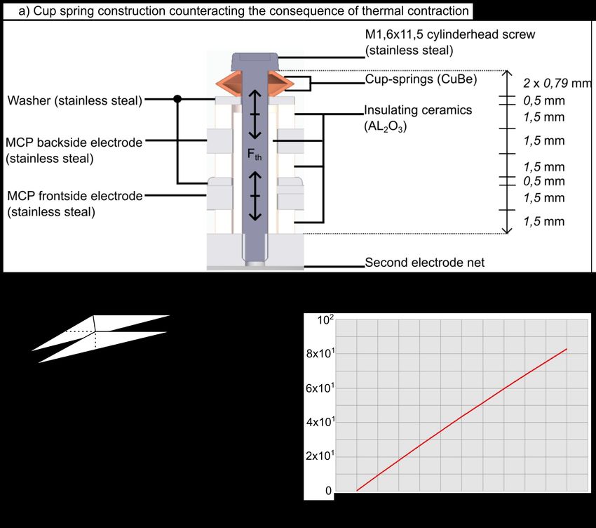
3.2.1. Cup Springs Counteracting the Consequence of
Thermal Contraction
The different thermal expansion coefficients of the insulating ceramics
and the A4-steel parts can lead to a problem during the cooling process.
Thermal contraction may cause tension across the channel plate due to
fabrication tolerances and local unevenness of different construction parts.
The original construction had to be adapted and additional CuBe cup
springs were integrated (see Figure 3.5). The length contraction for the
different materials can be calculated according to Equation 2.13 using
the thermal expansion coefficients αSteel = 16 · 10−6 /K for stainless steel
and αAl2 O3 = 11 · 10−6 /K for the insulating ceramics. These used room
temperature values are taken from the Solid Works data base and change
during the cooling process. The relevant temperature range reaches from
room temperature (300 K) to around 10 K, yielding ∆T = 290 K. The
length of materials relevant for different contraction is 4.5 mm (see Figure
1
Common stainless steel is called A2-steel. Compared to that, A4-steel contains a few
percent of molybdenum to further improve its oxidation properties.22 3. Microchannel Plate Detectors
Figure 3.5.: Characteristics and working principle of CuBe cup springs, used to
partially absorb the thermal contraction. a) Modified construction. The screw,
the electrodes and the washers are made of A4 stainless steel, while the insulating
ceramics are made of Al2 O3 . Due to different thermal expansion coefficients
one has to oppose the change in length of a total of 4.5 mm ceramics to that
of stainless steel. The cup spring provides a force counteracting to the thermal
contraction Fth . b) Relevant parameters of the cup springs. c) Response curve,
generated using [31]. The spatial dimensions used can be seen in (b), the Poisson
number is 0.37, taken from the Solid Works data base.
3.5). These relevant parts are where the screw is surrounded by insulating
ceramics.
Stainless steel : ∆Lscrew ≈ 21 µm, (3.6)
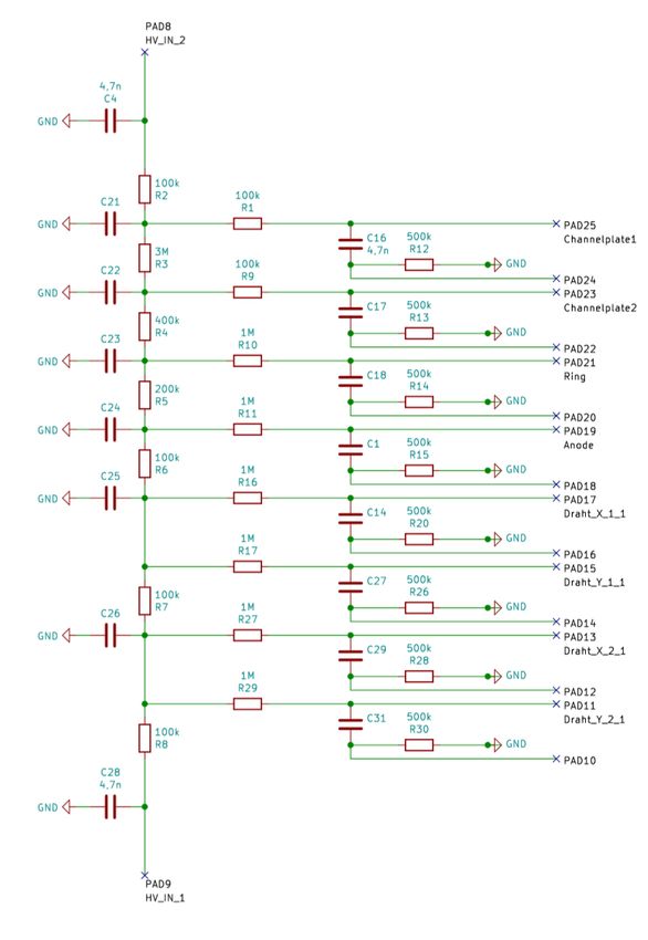
Al2 O3 −ceramics : ∆Lceramics ≈ 14 µm. (3.7)3.2. MCP Detector Construction 23 Since the screw is contracting more than the ceramics, the cup-springs have to compensate a total length contraction of ∆Ltot ≈ 7 µm. Comparing this result to Figure 3.5.c) the counteracting force per cup spring yields about 14 N. Using a total of 32 springs and considering the stacking of two springs per screw the final counteracting force results in 112 N. 3.2.2. Voltage Supply To provide proper voltages (complete scheme shown in Figure 3.6) a first Voltage Distribution Box (VDB) is used respectively a voltage divider (circuit diagram see Appendix A). It distributes a single input voltage to separate, independent outputs supplying the MCP front and back electrode, the anode ring and the anode wiring. One uses a series of voltage dividers, its resistors were chosen such that a positive voltage gradient is built up from the MCP front face towards the anode. The first and second electrode net is contacted separately via two further voltage supplies. Thus, the voltage gradients accelerating incoming particles and SEM electrons are decoupled such that the detector can be used for positively or negatively charged particles. Also, the voltage applied to the first electrode net can be chosen freely such that it can be adapted to the electric field gradient inside the reaction microscope [8; 9; 10]. The Double Dealy Line (DDL) anode consists of one long, alternately winded signal and reference wire, both for x- and y-direction. The delay line-outputs of the first box are connected to a second VDB (circuit di- agram see Appendix A) where the four inputs (XSignal , XReference , YSignal and YReference ) are split into eight outputs, two for each input (for example X1,Signal and X2,Signal ). These outputs are connected to the wires of the double delay line where X1,Signal and X2,Signal denote the starting respec- tively ending point of the signal-wire in x-direction. A correct connection of signal and reference in- and outputs is important, because VDB 1 provides slightly higher voltages to its signal outputs X1,1 and Y1,1 . Thereby, one achieves that more SEM electrons collide with the signal wires. The final signal outputs of the second VDB X1 , X2 , Y1 and Y2 denote noise free, decoupled, low voltage subtraction signals X/Y1/2 = X/Y1/2,S − X/Y1/2,R . Now “Signal” and “Reference” is abbreviated by “S” and “R”. These signals are used for data acquisition.
24                                          3. Microchannel Plate Detectors

Figure 3.6.: Used voltage distribution principle. A high voltage supply is
connected to the HV-In-2 connector of Voltage Distribution Box 1 (VDB 1).
Using a series of voltage dividers, the input voltage is fractionized (circuit diagram
see appendix A). While the ring electrodes of the detector are connected directly
to VDB 1, the double delay line needs a second VDB. This box guides its four
inputs to eight outputs by splitting up one input into two identical outputs
(circuit diagram see appendix A). One connects the two ends of one signal ( i.e.
X1,S and X2,S ) and one reference wire (i.e. X1,R and X2,R ) of the double delay
line for x- and y-direction. During measurements these outputs also act as signal
inputs. The decoupled subtraction signals X/Y1/2 = X/Y1/2,S − X/Y1/2,R are
further processed in the data acquisition. The lowered voltage signal of one of
the two MCP electrodes is needed for triggering the data acquisition.

  The complete voltage distribution scheme can be seen in Figure 3.6. The
separate voltage supplies for the detector nets are not shown. For wiring
3.3. Readout Technique and Data Acquisition                                                    25

the double delay line it is necessary to use a twisted pair configuration2
connecting related ends of signal and reference wires. Thereby the influence
of external high frequency signals can be minimized with low effort.

3.3. Readout Technique and Data Acquisition
In the following, the generation of a two dimensional image, extracted from
the electrical signals thumbed at the two ends of each wire, will be discussed.
For simplification it will only be referred to one exemplary DDL wire.

   The SEM electron cloud emitted from an MCP channel collides with the
wire of the DDL. Due to the clouds spatial extent more than one winding
can be hit. The electrons absorbed by the wire produce an electric pulse
traveling to both wire ends (see Figure 3.7). Due to broadening effects
caused by dispersion3 the signals do not consist of separate pulses for
numerous wires hit by the electron cloud emitted by one MCP channel for
one SEM reaction cascade. The outgoing signals are in the first instance
processed in VDB 2. The inductive decoupling produces a positive signal
according to X/Y1/2 = X/Y1/2,S − X/Y1/2,R . Hence, background noise is
prevented and the carrier voltage becomes zero.
   Since the used amplifier Ortec FTA 820 only processes negative signals, an
inverter is added after VDB 2. The amplified signals are further processed
with an Analog Digital Converter ADC, provided by RoentDek. The four
signals X1/2 and Y1/2 , as well as the MCP signal define the inputs of the
ADC. During a reaction cascade inside a MCP channel, charge is depleted
of the channel wall. Thus, the voltage drops for the duration of the SEM
cascade and is restored by the voltage supply. This voltage drop is the origin
of the data processing, it is used as group trigger for the delay line channels.
Once the MCP-signal intersects the trigger threshold at time tTrigger−1 a
time window [tTrigger−1 − 14.4 ns; tTrigger−2 + 19.2 ns] is opened to sample
the delay line channels, whereas the positive time limit is determined after
the MCP signal falls below the trigger threshold at time tTrigger−2 again.
 2
     A twisted-pair-configuration is simply achieved by twisting the cables.
 3
     Similar to laser pulses in refractive media, electrical pulses suffer from dispersion effects.
      Different frequencies experience different drift velocities and the pulse broadens as
      the signal “collects” additional group delay dispersion during propagation.
26 3. Microchannel Plate Detectors
Figure 3.7.: Working principle for the production of signal pulses for a single
DDL wire. (a) The electron cloud hitting the wire produces an electrical pulse
traveling to both wire ends where the signals V1 and V2 are thumbed. (b) Before
the decoupling, the carrier voltage equates to the voltage V0 applied to the DDL.
In the analysis each pulse is assigned to the time t1/2 which refers to its electrical
propagation time.
In this time window all incoming and already digitized signals are saved
if their amplitude is higher than their individual trigger threshold which
can be set for each channel independently. For each signal the amplitude
A and its point in time ts with respect to the calculated time of the MCP
voltage drop tMCP is determined as shown in Figure 3.8. Using the time
sum condition
tx/y,1 + tx/y,2 = const, (3.8)
one can assign related signals. The spatial representation is finally calculated
by:
X/Y = fx/y · tx/y,2 − tx/y,1 , (3.9)
with the proportionality factor fx/y which represents the vertical drift ve-
locity for signals on the delay line.
In case of lost signals, one can fall back to different reconstruction
algorithms using the time sum. Also two MCP signals which are produced by
coincident particles, can be separated by a deconvolution algorithm, as long3.3. Readout Technique and Data Acquisition 27 as the Rayleigh limit ∆t ≥ 1.22·FWHM is fulfilled where ∆t is the temporal separation of the two timestamps and FWHM describes the larger of the two Full Width Half Maxima of the signals. Due to the mostly qualitative scope of this work, the shown analysis is sufficient. For experiments using a reaction microscope further reconstruction principles will potentially become important, more detailed information can be found in the Ph.D. theses of Senftleben [32], Schnorr [33] and Pflüger [34]. Although they used a different data acquisition system, the principle of various reconstruction algorithms can be integrated to various data acquisitions. Figure 3.8.: Schematic of signal processing. After digitizing an incoming pulse, it is in a first instance characterized by three parameters: the maximum amplitude of the signal A, A50 = A/2 and the time ts . The amplitude is determined by the maximum of a parabola, fitted to the three highest bins of the signal. The second step is calculating A50 . The four nearest signal bins of A50 define a Bézier spline which intersection with the A50 -line yields the signal’s point in time ts . Since real signals can look much more jittery than shown here, it is more reliable to use the Bézier spline to determine a timestamp than just to use the maximum of the fitted parabola.
4. Experimental Setup
The setup inside the vacuum chamber is shown in Figure 4.1. Each flange
with diameter d ≥ 40 mm is sealed with viton o-rings, suitable for pressures
down to 10−10 mbar. To achieve temperatures in the few Kelvin regime i.e.
to isolate the detector from ambient thermal radiation two thermic shields
are installed and thermally connected to the two stages of the coldhead.
The shields are made of high purity copper which has an emissivity  of
0.02 (polished) to 0.05 (untreated, shining). Incident black body radiation,
caused by construction parts at room temperature (T0 = 300 K), transfers
heat to the system. The heat input reads:

                              Q̇ = κB s As T04 − Ts4 ,                        (4.1)

   with the emissivity s , the Stefan Boltzmann constant κB = 5.67 W2 /m2 K4 ,
the actively reflecting area As and the temperature Ts of the shield. Assum-
ing Ts = 30 K, using s = 0.05 and As = 0.2 m2 it yields Q̇ ≈ 4.6 W. By
comparing this result to the capacity map (see Figure 4.2), provided by
Sumitomo, one sees that the beforehand used assumption of Ts = 30 K is
valid. When the temperature of stage 2 is in the region of a few Kelvin,
the outer shield (thermally equivalent to stage 1) is cooled with a power of
around 5 W at 30 K. This leads to an equilibrium between input heat and
cooling power and the temperature of the shield stays constant. When the
shield reaches sufficiently low temperatures, single constituent elements of
air start to condensate e.g. nitrogen condensates at surrounding conditions
of 77 K and 1 bar1 . This condensate layer influences the emissive properties
of thermic shields and can increase the external heat input [36]. Addition-
ally to the copper shields themselves, the lower part of the outer shield
is wrapped with multilayer insulation (10 layers). This further improves
the emissive properties and therefore decreases external heat input. In
 1
     With decreasing pressure the condensation temperature decreases. Please find the
     p-T-diagrams for a couple of elements and molecules in Day [35].

                                          28
29
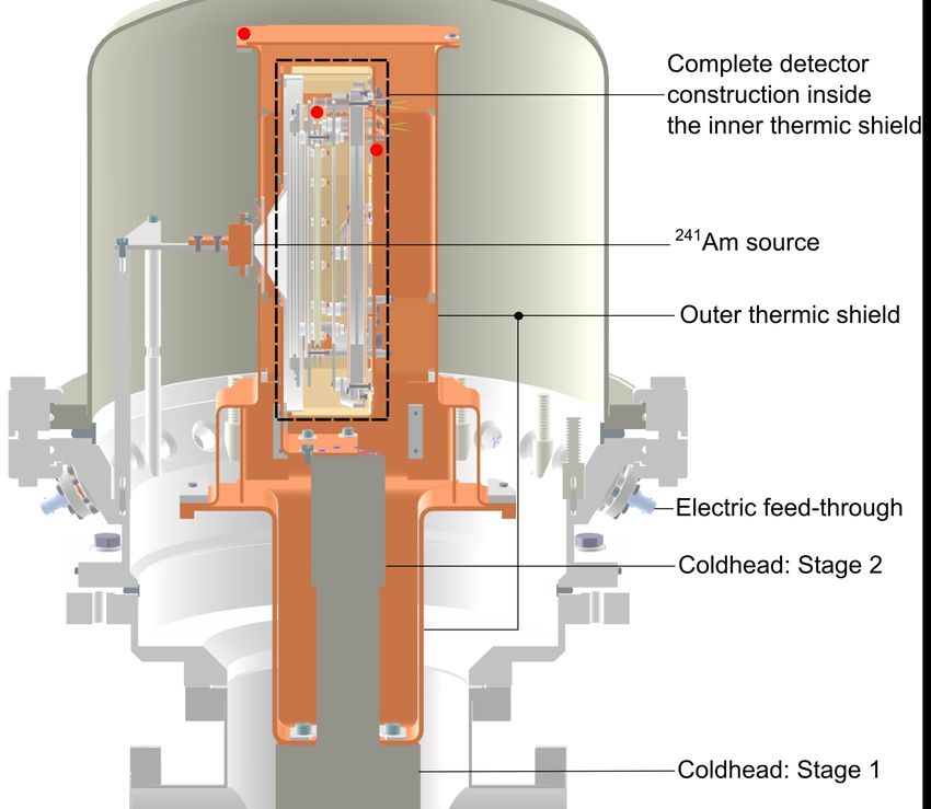
Figure 4.1.: Profile of the measurement setup. The coldhead is fixed on the
bottom of the vacuum chamber. The outer thermic shield is mounted on stage
1 of the coldhead while the inner thermic shield is mounted on stage 2. Hence
both shields are in thermal equilibrium with the respective stage. The detector
is located inside the inner shield. The 241
95 Am-source is mounted separately on
a non-shielded attachment and stays unaffected by the cryo temperature. The
positions of three Si-diodes for temperature measurements is marked with red
spots.
Equation 4.1 only the copper parts without multilayer insulation are taken
into account.
Pt1000 elements, type K thermocouples and Si-diodes are used for tem-
perature measurements. One Pt1000 and one thermocouple is mounted at30 4. Experimental Setup Figure 4.2.: Capacity map of the coldhead model RDK-408D2, produced by Sumitomo, at 50 Hz-operation, taken from [37]. The horizontal lines describe the heat pumping power of stage 2, the vertical lines the heat pumping power of stage 1. The x- and y-axis shows the temperature of stage 1 and stage 2, respectively. The pumping powers of the two stages are strongly correlated, e.g. it is not possible to cool one stage independently. The region of interest is marked in red, desirable temperatures would be 30 K at stage 1 and 10 K at stage 2. the top of the outer shield and one of each of these three types on the foot of the inner shield which is directly screwed to the second stage of the coldhead. One further thermocouple is mounted on the frontside of the source holder and one further Si-diode is placed on the MCP frontside electrode. By this extensive use of sensors the temperature of all relevant parts of the experimental setup can be tracked. Due to the high precision of Si-diodes in the cryogenic temperature range, most temperatures presented in this work are taken from these sensors. For sufficient thermal conductivity between different construction parts which belong to the same thermal stage each
31

contact point is coated with a thin layer of Apiezon N. This film provides
reliable thermal contact of separate parts.
32                                               4. Experimental Setup

4.1. List of Used Devices

 Purpose                  Device                    Comment

 Fore-Vacuum Controller   Leybold IoniVac
                          IM 540
 Fore-Vacuum Gauge        Leybold Thermovac         Used twice,
                          TTR 91 NS                 pmin               =
                                                    3.8 · 10−4 mbar
 UHV-Controller           Vacom ATMIGRAF
 UHV-Gauge                Vacom ATMION              pmin = 1 · 10−10 mbar
 Turbo Controller         Pfeiffer DCU 110          Used for HiPace 80
 Turbo Pump               Pfeiffer HiPace 80
 Turbo Controller         Pfeiffer DCU 310          Used for HiPace 300
 Turbo Pump               Pfeiffer HiPace 300
 Fore-Vacuum Pump         Edwards nXDS6i
 Coldhead                 Sumitomo                  Stage 1: 40 W @ 43 K
                          RDK 408 D2                Stage 2: 1 W @ 4.3 K
 Compressor               Sumitomo
                          CSW 71
 Temperature Controller   CryoCon 24 C
 Si-Diode                 CryoCon S950              Used threefold for
                                                    temperature measure-
                                                    ment
 Amplifier                Ortec FTA 820             Gain G = 200
 High Voltage Supply      NHQ 204 M (2x)
                          NHQ 206 L (1x)
 Voltage Supply           Rhode & Schwarz           Used for heating
                          HMP 4040                  resistor
 Oscilloscope             Rhode & Schwarz
                          RTM 3004
 Data Acquisition         RoentDek
                          FADC 8B/10-2

                    Table 4.1.: List of used devices.
4.2. Alpha Source and Effective Solid Angle 33
4.2. Alpha Source and Effective Solid Angle
The particle source is 241 95 Am with an activity of A0 = 37 kBq at the
production day (7th December 1971). Its primary decay path with a half
life of T1/2 = 432.6 a [38] is:
95 Am 93 Np + α ( + γ ), (4.2)
241 237
→
where α and γ describe a 42 He-core and a photon, respectively. With a
probability of 85% an energy of 5.486 MeV is released. Additionally to the
alpha particle in most of these reactions one or more gamma quanta are
produced. Using the decay law
dN
= −λdt, (4.3)
N
one can determine the activity in the year 2020 to be
ln(2)
!
A(t) = A0 exp − t = 34.2 kBq, (4.4)
T1/2
emitted into a solid angle of 4π. In the next step the effective solid angle of
the MCP is calculated. The distance between source and MCP is x = 39 mm
and the effective MCP radius is a = 55 mm (see Figure 4.3). Assuming a
pointlike source the half apex angle of the included cone is α = 0.954 rad.
Thus the effective solid angle Ω reads
Ω = 2π (1 − cos(α)) = 2.649 sr. (4.5)
Hence, the effective rate of emitted alpha particles, seen by the MCP, results
to
AMCP = 7.22 kBq. (4.6)
In reality the source has a diameter of 7 mm and hence a spatial extent, this
can slightly increase the effective solid angle and the calculated effective
activity. Also the emitted photons and provoked ions from the MCP front
face can produce SEM cascades and have to be taken into account. In
contrast to that the transmission of the electrode nets and the OAR of the
detector decrease the measured rate.34 4. Experimental Setup
Figure 4.3.: Determination of the relevant solid angle. The distance between
the MCP and the 241
95 Am-source is x = 39 mm, the MCP has an active radius of
a = 55 mm. This yields the half apex angle of α = 0.954 rad.
4.3. Thermal Connection towards the MCP
In this section two optimizations of the thermal connection towards the
MCP are discussed. These changes to the original setup lower the minimally
reachable MCP temperature to 35 K. Additionally, possibilities for further
optimization are presented.
During the process of building up the setup, it became clear that the
thermal connection between the second stage of the coldhead and the
detector is insufficient. The only direct connection between the baseplate of
the detector and the coldhead is made up of four screws out of stainless steel
(see Figure 4.4). These stainless steel-copper junctions are inappropriate to
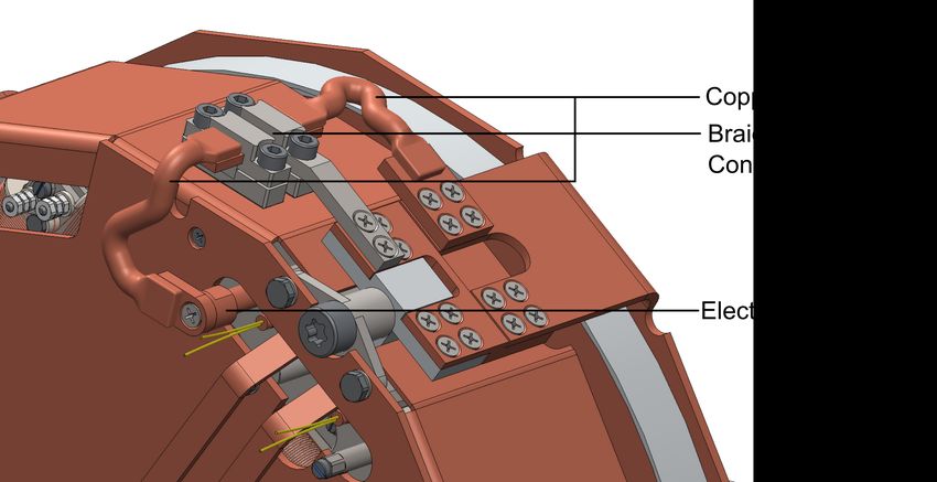
transport enough heat from the detector towards the coldhead which yields a4.3. Thermal Connection towards the MCP 35 low effective cooling power. After four days of cooling, the baseplate adapted to a temperature of 33 K while the second stage equilibrated at 6.5 K after one day of cooling. Additionally, there are further steel-ceramic-junctions (separating the different detector modules, see Figure 3.4) decreasing the effective cooling power for the MCP. Of course, the setup will equilibrate at some point but to provide measurement results within proper times the timescale of cooling down the detector had to be lowered. Figure 4.4.: Construction of the inner shield including the detector. The four stainless steel screws, marked as “Steel-Copper-Junctions”, define the only direct connection between the second stage and the detector baseplate before the improving copper braid construction (see Figure 4.5) is added. To improve the thermal conductivity between the MCP and the coldhead a copper braid is added. It thermally connects the part of the inner thermal shield which is directly mounted to the coldhead, and the MCP front face electrode (see Figure 4.5). Due to the high voltage difference between the
36                                                         4. Experimental Setup

MCP electrode and the thermal shield (ground potential) both have to
be electrically decoupled. Therefore, a sapphire crystal2 is added between
the two parts of the braid (see Figure 4.5) such that electrical safety can
be guaranteed. It is also important that different parts of the additional
construction have to be connected using surfaces which are as large as
possible. A bigger contact surface increases the thermal conductivity
between single parts.

Figure 4.5.: Improving the thermal conductivity between the second stage and
the channel plate. For best possible results the electrode connector and the
screw fixing the lower part of the braid is produced out of copper instead of
A4-steel. To achieve the electric decoupling two single braid parts are separated
by a sapphire. The lower part of the braid which is electrically contacted to the
MCP electrode has to be isolated by numerous short ceramic pipes to prevent
direct electrical contact to other construction parts. The upper part of the braid
was redesigned to a solid copper part before the measurements were executed.

   After an additional temperature sensor has been added to the MCP
front face electrode using a cryo-suitable epoxy adhesive (Stycast FT 2850
combined with the Stycast Catalyst 9), the temperature was recorded during
the cooling process. The measured temperatures and MCP resistances of
 2
     Artificial sapphires have a very high thermal conductivity and act electrically as
      insulators.
4.3. Thermal Connection towards the MCP 37
the first cooling process with copper braid is shown in Figure 4.6. The
MCP resistance is determined using a voltage divider. A resistor with
Rin = 500 kΩ is connected in parallel to the MCP stack and a supply
voltage of Uin = 500 V is applied. By measuring the dropped voltage Uout
of the additional resistor the MCP resistance can be calculated:
Uin
RMCP = Rin −1 . (4.7)
Uout
Figure 4.6.: Temperatures at different positions (left) and MCP resistance
(right) during the first cooling process after installing the Cu-braid. The left side
shows the temperatures at the MCP front face electrode (blue), at the detector
base plate (red) and on top of the second stage of the coldhead (black). Since
the material inside the inner shield has to be as cold as possible, the blue curve
is most relevant. At the end of the curves the final temperatures are shown
as displayed by the temperature controller. The precision of the temperature
measurement is 0.5 K. The minimal temperature reached at the MCP front face
is 44.62 K. The right side shows the calculated MCP resistance (Equation 4.7)
using Uin = 500 V and Rin = 500 kΩ. From this one can see that for the final
MCP front face temperature the MCP resistance is measured to be 1.1 GΩ.
Since the final temperature at the MCP front face after more than 60 h of
cooling was measured3 to be 44.62 K, further improvements had to be made.
3
The precision of the temperature measurement is 0.5 K. The discussed values are
taken as displayed by the temperature controller.You can also read