Electrically Transduced Gas Sensors Based on Semiconducting Metal Oxide Nanowires - MDPI
←
→
Page content transcription
If your browser does not render page correctly, please read the page content below
sensors
Review
Electrically Transduced Gas Sensors Based on
Semiconducting Metal Oxide Nanowires
Ying Wang 1 , Li Duan 2 , Zhen Deng 3, * and Jianhui Liao 4
 1    Key Laboratory of Luminescence & Optical Information, Ministry of Education, School of Science,
      Beijing Jiaotong University, Beijing 100044, China; yingw@bjtu.edu.cn
 2    Beijing Key Laboratory of Security and Privacy in Intelligent Transportation, Beijing Jiaotong University,
      Beijing 100044, China; duanli@bjtu.edu.cn
 3    Key Laboratory for Renewable Energy, Beijing Key Laboratory for New Energy Materials and Devices,
      Beijing National Laboratory for Condensed Matter Physics, Institute of Physics,
      Chinese Academy of Sciences, Beijing 100190, China
 4    Key Laboratory for the Physics and Chemistry of Nanodevices, Department of Electronics,
      Peking University, Beijing 100871, China; Jianhui.Liao@pku.edu.cn
 *    Correspondence: zhen.deng@iphy.ac.cn; Tel.: +86-010-8264-9296

 Received: 27 October 2020; Accepted: 23 November 2020; Published: 27 November 2020

 Abstract: Semiconducting metal oxide-based nanowires (SMO-NWs) for gas sensors have been
 extensively studied for their extraordinary surface-to-volume ratio, high chemical and thermal
 stabilities, high sensitivity, and unique electronic, photonic and mechanical properties. In addition
 to improving the sensor response, vast developments have recently focused on the fundamental
 sensing mechanism, low power consumption, as well as novel applications. Herein, this review
 provides a state-of-art overview of electrically transduced gas sensors based on SMO-NWs. We first
 discuss the advanced synthesis and assembly techniques for high-quality SMO-NWs, the detailed
 sensor architectures, as well as the important gas-sensing performance. Relationships between
 the NWs structure and gas sensing performance are established by understanding general
 sensitization models related to size and shape, crystal defect, doped and loaded additive, and contact
 parameters. Moreover, major strategies for low-power gas sensors are proposed, including integrating
 NWs into microhotplates, self-heating operation, and designing room-temperature gas sensors.
 Emerging application areas of SMO-NWs-based gas sensors in disease diagnosis, environmental
 engineering, safety and security, flexible and wearable technology have also been studied. In the end,
 some insights into new challenges and future prospects for commercialization are highlighted.

 Keywords: semiconducting metal oxide; nanowires; gas sensor;                            sensing mechanism;
 doped/loaded additive; crystal defect; low-power consumption

1. Introduction
     Rapid and real-time detection of toxic, flammable and explosive gases at low concentrations
is essential in various areas like environmental protection [1–4], chemical analysis [5,6], safety and
security [7–9], diagnosing diseases [10,11]. Each year, gas fires and explosion accidents in kitchens occur
all over the world, causing heavy losses to personal property and life safety. Thus, methane sensors
are the mandatory equipment in many countries to give alarm signals when the concentration of
methane reaches the explosive limit. High-sensitive gas sensors are also required to detect air
pollutants like nitrogen oxides (NOx ) and formaldehyde (HCHO), which are produced abundantly
by industrial production and interior decoration. Medical studies have recently shown that breath
sensors can be translated into clinical diagnostics by monitoring certain volatile organic compounds

Sensors 2020, 20, 6781; doi:10.3390/s20236781                                        www.mdpi.com/journal/sensors
Sensors 2020, 20, 6781                                                                               2 of 41

(VOCs) because they can act as biomarkers for some chronic diseases [12,13]. It is generally
believed that the breath of lung cancer patients contains a large amount of benzene series (toluene,
xylene, etc.) [14–16], and the breath of diabetes patients contains a higher concentration of acetone
(>1 ppm) [17,18]. Gas sensors have become an indispensable part of the modern Internet of things
(IoT). According to a recent market analysis report, the global gas sensor market is anticipated to
reach USD 4.1 billion by 2027 [19]. Therefore, many sensing technologies including the infrared
spectroscopy [20], gas chromatography [5,21], colorimetry [22], surface plasmon resonance [23],
surface acoustic transducer [24], cantilever [25], electrochemistry [26,27], and capacitor [28], have been
developed for high-performance gas sensors. Compared with the above optical, chemical, acoustic or
gravimetric sensors, a class of electrically transduced gas sensors are attractive for their rapid and
real-time detection, simplicity, miniaturization, portability, the possibility of continuous monitoring,
and compatibility with standard electronic equipment.
      There are two important aspects in an electrically transduced gas sensor: the sensor architecture
and the sensing material. On one hand, electrical parameters (resistance, current, voltage or capacitance)
can be measured with different sensor architectures, including chemiresistor, field-effect transistor
(FET), diode, chemical capacitor, and electrochemical device. Of these, a chemiresistor consisting
of only two electrodes is the most commonly used, and FET sensor configuration with the current
modulated by the extra gate electrode is generally regarded as a good platform to study the gas-sensing
mechanism. On the other hand, the sensing material is responsible for interacting with the target
gases and transforming the chemical signals into electrical signals. Semiconducting metal oxides
(SMO) such as stannic oxide (SnO2 ) [29,30], zinc oxide (ZnO) [31,32], tungsten oxide (WO3 ) [33,34],
copper oxide (CuO) [35,36], indium oxide (In2 O3 ) [37,38], nickel oxide (NiO) [39,40] and titanium
oxide (TiO2 ) [41,42], are generally regarded one class of the most promising sensing materials for their
chemical stability, simple processing, low cost, and high sensitivity performance.
      The rapid development of innovative nanomaterials and technologies has promoted the progress
of gas sensors since the end of the 1990s. Compared with bulk SMO and their sputtered thin
films, one-dimensional nanowires (NWs) offer many advantages for gas sensors, such as high
surface-to-volume ratios, Debye lengths comparable to the target gas molecules for superior
sensitivity, excellent thermal stability, relatively low power consumption, and low tendency to form
aggregates [43–46]. Till now, SMO-NWs with various sizes, shapes and compositions can be synthesized
by physical deposition and vapor/liquid-phase chemical processes [47–49]. Assembling strategies
like dip-coating, printing, Langmuir–Blodgett (LB) technique, and template assembly have been
developed for the alignment of NWs on various substrates [50–54]. Moreover, site-specific growth
and in situ integration of NWs have been studied towards large scale fabrication of commercialized
sensor products [35,37,55,56]. Modern synthesis and assembly methods allow unprecedented control
of structural properties, and yet, the sensing mechanism is still confusing.
      The nature of the fundamental operating principle of SMO gas sensors is described as the surface
reaction of target gases with ionsorbed oxygen. Here we take the SnO2 NW-based chemiresistor as an
example [30,57–59]. Under ambient conditions, oxygen molecules in air adsorb on the active sites of
SnO2 surface and accept electrons from the conductance band of SnO2 to form oxygen ions (O− , O2 − ,
or O2− ). The consumption of electrons in this process leads to a depletion region, the depth of which
is known as the Debye length. When the SnO2 NW sensor is exposed to a reducing gas like ethanol
(C2 H5 OH) or carbon monoxide (CO), the reducing molecules react with the surface oxygen ions and
release electrons back to SnO2 so that the sensor works at a lower resistance state. The Debye length (L)
is typically on the order of 2–100 nm [60]. Thus, it is likely that electrons can be exhausted for NWs with
small diameter (D), leading to high sensitivity to reducing gases, especially when D is comparable to or
less than 2L (D-L model achieved by the Yamazoe group [61]). In contrast, some studies have reported
that crystal defects in SMO-NWs can significantly affect the gas-sensing performance, which makes
the conventional D-L model invalid [62–65]. The development of in situ and in operando methods
plays a key role in giving detailed sensing mechanisms instead of empirical explanations [64,66,67].
Sensors 2020, 20, 6781                                                                             3 of 41

Moreover, based on the significant theories proposed by Yamazoe and Morrison in the 1980s [68,69],
Degler et al., has recently provided revised concepts for understanding the fundamental mechanisms
of doped and loaded additives on SMO-based gas sensing materials [70]. The gas response of an
SMO-NWs sensor can also be attributed to contact effects, including both the intra-NW junctions
and the electrical contacts [71–73]. Instead of finding a correlating model to explain the experimental
findings, we focus on the comprehensive survey of the relationship between the materials’ structure
and gas sensing performance.
     A number of developments in low-power sensing technologies and novel applications have been
extensively explored, which are associated with the battery-driven IoT. One well-known challenge
of SMO gas sensors is that they usually work at relatively high temperatures of 200–400 ◦ C [74–77].
The high power dissipation limits their practical application. Therefore, many studies have attempted
to lower the operating power of SMO-NWs gas sensors, the methods of which can be described
as thermal isolation, self-heating operation and developing room-temperature sensors [4,58,78–82].
Moreover, recent advances in the fabrication and integration of SMO-NWs offer unique possibilities
for their application in on-chip sensor arrays, flexible sensors and even smart textiles [45,83–86].
These innovations are critical to further progress in IoT-based projects such as smart homes,
telemedicine and safe driving.
     Although several recent reviews have been published concerning one-dimensional nanostructure-
based gas sensors, most of them focused on other NWs like carbon nanotube, metal, silicon, GaN and
polymer [87–92]. The latest comprehensive review on SMO-NWs-based gas sensors is still lacking
considering the quickly evolving technologies in this area. In this review, we intend to describe
investigations on SMO-NWs and their electrically transduced gas sensors by highlighting the most
significant processes related to synthetic methodology, assemblies, fundamental structure–property
correlations, strategies for low power consumption and novel applications.

2. SMO-NWs: Synthesis, Assembly and Sensory Device
      According to the dominant charge carriers, SMO-NWs can be classified into n-type NWs
(like ZnO, SnO2 , In2 O3 , WO3 and TiO2 ) and p-type NWs (like CuO and NiO). For n-type SMO-NWs,
oxygen adsorption causes an electron depleted surface layer, and for p-type SMO-NWs, it causes
a hole accumulated layer. Based on the Boltzmann statistics [93,94], the resistance change in the
case of an accumulated layer is much smaller than the one corresponding to the depletion layer.
Hole mobilities are often very low in p-type oxides (0.2 cm2 V−1 s−1 for NiO) [44]. In contrast, SnO2 and
ZnO NWs with high electron mobility (160 and 200 cm2 V−1 s−1 , respectively) are highly sensitive
materials [46,70,95]. These are the two reasons why p-type SMO-NWs are less used compared to n-type
ones, especially for detecting oxidizing gases. However, p-type SMO-NWs are also important topics in
gas sensor research because of their low-temperature dependence, high humidity or thermal stability,
and a high potential for p-n junction applications [73,96]. Typically, CuO is one of the key p-type
SMO materials that have been extensively investigated for reducing gases like CO [73,97–99]. In this
section, a discussion is organized to cover the SMO-NWs synthesis, assembly, sensor architecture,
and important performance parameters.

2.1. Synthesis of SMO-NWs
     The controllability of ZnO microstructures was demonstrated as early as 1971, using a vapor-phase
method [100]. In the late 1990s, Yang and Lieber reported a series of studies on the laser ablation
and vapor–liquid–solid (VLS) growth of crystalline SMO-NWs [101]. Moreover, Li et al., reported
ordered ZnO NW arrays fabricated by electrodepositing and oxidizing Zn in porous anodic alumina
membranes (AAM), which was later described as the template-assisted growth in liquid [102]. Till now,
there are many different methods in synthesizing SMO-NWs. Considering the large volume of research
work, we selectively present the most prominent methods that can be classified into the strategies of
top–down and bottom–up.
Sensors 2020, 20, 6781 4 of 41
The top–down preparation techniques obtain NWs from SMO thin films through combined
lithographic methods with physical or chemical depositions [98,103–106]. In this case, SMO-NWs
can be directly incorporated into a sensor circuit without an additional assembly step. The precise
position, aligned structure and highly uniform dimensions also benefit the integration of NWs
into multifunctional devices. However, the challenge for top–down techniques is that it becomes
increasingly difficult to fabricate regular NWs in nanoscale dimensions. For example, Cho et al.,
prepared a well-aligned PdO NW array using the lithographically patterned Pd NW electrodeposition
followed by subsequent thermal oxidation [103]. The PdO NWs are 150 nm in diameter, while the
NW edges are irregular and intermittently interconnected with poor electrical conductivity. Using a
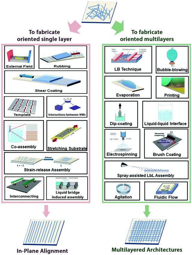
textured growth substrate can achieve NWs with smaller diameters. Recently, aligned vanadium
oxide (VO2 ) NWs with tunable lateral dimensions of 20–690 nm are produced after heating V2 O5 thin
films on a grooved silicon oxide (SiO2 ) surface, which is based on a directional Ostwald ripening
process (Figure 1a,b) [105]. The high-resolution transmission electron microscope (HR-TEM) image
in Figure 1c shows the marked lattice spacing of 0.467 nm corresponding to the interplane spacing
of the (010) and (001) planes of monoclinic VO2 crystals. The significant changes in Raman spectra
with increasing annealing temperature also demonstrate that the V2 O5 is converted to VO2 at 700 ◦ C
for 30 min (Figure 1d). In contrast, additional transfer of VO2 NWs onto other substrates is necessary
before fabricating sensor devices. It is also challenging to fabricate single crystalline SMO-NWs by
top–down methods.
Figure 1. Directional Ostwald ripening for producing aligned arrays of VO2 nanowires (NWs).
(a) Ex situ scanning electron microscope (SEM) images of morphological evolution of the VO2 as a
function of temperature and growth time. Scale bar: 1 µm. (b) SEM images with the angle of the
V-groove 70◦ . Scale bar: 1 µm. (c) HR-TEM image of the VO2 NW. Scale bar: 5 nm. (d) Raman spectra
obtained with the laser incident on the V-grooved surface. Reprinted from reference [105] with
permission from the American Chemical Society.
By contrast, the bottom–up techniques assemble atomic or molecular precursors into NWs
through a vapor phase or a liquid phase process, which offer several advantages such as flexibility,
low cost and simplicity. Vapor-phase synthesis is generally performed inside a horizontal tube
furnace under appropriate conditions of source, substrate, catalyst, temperature, pressure and gas
flow [101,102,106–114]. The growth mechanism can be well defined by vapor–liquid–solid (VLS),
vapor–solid (VS), vapor–solid–solid (VSS), oxide-assisted growth or self-catalytic growth [47,107,108].
In recent years, many efforts have been devoted to the rational design for improving the crystal quality,
reducing growth temperature of SMO-NWs and growing NWs on amorphous substrates. Takeshi’s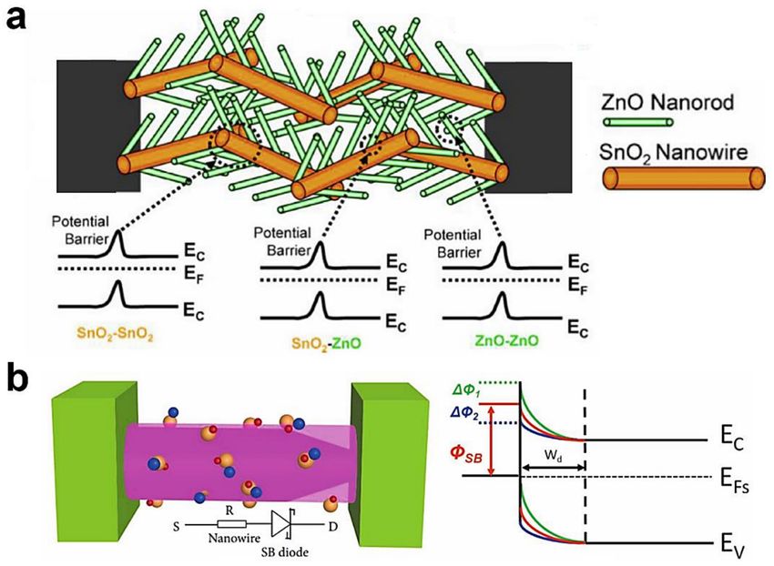
Sensors 2020, 20, 6781                                                                                5 of 41

group provided the concept of temperature-dependent “material flux window”, and successfully
fabricated SMO-NWs like magnesium oxide (MgO), SnO2 and ZnO on polyimide substrates at relatively
low growth temperatures [112,113]. Recently, Güniat et al., have given impressive insights on the
vapor-phase synthesis of NWs [108]. They have summarized the open questions to be explored,
such as reducing the size distribution, understanding the microscopic interaction of the NW interface,
explaining the defect formation, etc. Correspondingly, liquid-phase synthesis and growth of SMO-NWs
are performed in chemical solutions. Typical process variations have been comprehensively discussed in
the case of liquid-phase synthesis, including hydrothermal, solvothermal, molten salt, template-assisted,
electrodeposition, and electrostatic spinning synthesis of SMO-NWs [57,115–119]. As shown in Figure 2,
Zhao et al., have recently succeeded to rationally synthesize monodispersed ZnO NWs from randomly
sized seeds by a two-step hydrothermal growth [120]. Figure 2c shows that the distribution of ZnO NW
diameters σ is around 1.3 nm; the best result to the authors’ knowledge. This proposed concept is also
of generality for other SMO-NWs and thus paves the way for NWs-integrated sensors with reliable
performance. Despite the tremendous progress, the main challenge for vapor-phase and liquid-phase
synthesis methods is the micro electro mechanical system (MEMS) compatible incorporation of NWs
on sensor circuits.

      Figure 2. Synthesis of monodispersedly sized ZnO NWs from randomly sized seeds. (a) Schematic
      illustration of the growth process. (b) SEM images of fabricated ZnO NWs. (c) The narrow diameter
      distribution of the two-step grown ZnO NWs. Reprinted from reference [120] with permission from
      the American Chemical Society.

      Towards the practical application of SMO-NWs, the integration of top–down and bottom–up
strategies is required to combine their merits. The first all-integrated sensor circuit based on
cadmium selenide (CdSe) and germanium/silicon (Ge/Si) NWs was reported by the Javey group
in 2008, showing the advantages of combining vapor-phase synthesis, printing and photolithography
techniques [121]. Moreover, Marasso et al., combined the top–down and bottom–up strategies
by developing a polymeric-mask centrifugation method to deposit ZnO nanostructures on MEMS
micro-hotplates [122]. Santra et al., reported the mask-less deposition of chemically synthesized
Au–SnO2 nanocomposites on MEMS platform through the use of dip-pen nanolithography (DPN) to
create a low-cost ethanol sensor [75]. Extensive studies have also focused on the local and site-specific
growth of SMO-NWs on microhotplates for on-chip integration [35,56,83,84,123,124]. On one hand,
in situ electrical and gas sensing measurements can be achieved for revealing new insights into sensor
degradation. On the other hand, NW-based electronic noses can be fabricated based on various
SMO-NWs materials combining chemical vapor deposition or electrostatic spinning (bottom–up) with
lithography technique (top–down).

2.2. Assemblies of SMO-NWs
     For sensor fabrication, NWs are usually deposited from a suspension in solution onto the
desired substrates. The early used drop-casting technique works well for studying the single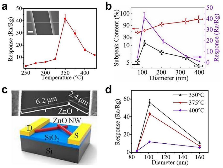
Sensors 2020, 20, 6781                                                                                  6 of 41

NW-based devices, but it can only lead to randomly assembled NWs with poor properties [64,125,126].
The controlled assembly of NWs into the aligned structure is necessary to produce large-scale and
high-performance NW-based gas sensors. To date, various assembly strategies have been developed
on various substrates. A very recent review paper by Hu et al., comprehensively presents the in-plane
aligned assembly of 1D nanoobjects [54]. They summarize the main techniques that lead to oriented
NW monolayers or multilayers, including assembly by external fields, shear coating, assembly by
template substrates, stretching of the substrate, Langmuir–Blodgett technique, evaporation-induced
assembly, contact printing, dip-coating, assembly at liquid–liquid interfaces, layer-by-layer assembly,
and so on (Figure 3). These techniques can be categorized based on the driving forces of template,
interface, interaction, external field, mechanical force and shear force that governs the oriented
assembly. Understanding the advantages and limitations of each method is necessary to choose the
best-suited strategy for ordered NW arrays with specific NW density, position, area, architecture and
alignment direction.

      Figure 3. Schematic illustration of assembling methods that can be applied to fabricate in-plane NW
      arrays and multilayer aligned NWs. Reprinted from reference [54] with permission from the Royal
      Society of Chemistry.

2.3. Electrically Transduced Sensing Architectures
     Most SMO-NWs are arranged in a horizontal direction. The architectures of electrically transduced
SMO-NWs gas sensors generally include chemiresistor, FET, diode, optoelectronic sensor, chemical capacitor
and electrochemical sensor, as shown in Figure 4. For SMO-NWs in this review, we particularly focus on
the general configuration and operation mechanism of chemiresistor and FET.
Sensors 2020, 20, 6781                                                                                   7 of 41

      Figure 4. Schematic illustration of electrically transduced gas sensors with semiconducting metal
      oxide-based nanowires (SMO-NWs) in the horizontal direction. NW, S, D, Vds , VG , A, C are short
      for nanowire, source electrode, drain electrode, bias voltage, gate voltage, ammeter and capacitance
      meter, respectively.

      A chemiresistor consists of two electrodes connected with sensing material, i.e., NWs assembled
or as grown on an insulating substrate. The change in resistance or current of the sensor device is
measured to analyze the concentration of the target gas. More than half of the reported gas sensors
are based on the chemiresistive architecture for their simplicity, compatibility with conventional DC
circuits, low cost and high accuracy. Notably, optoelectronic chemiresistors have attracted considerable
attention for their enhanced sensing response by creating photo-generated carriers participating
in the surface reaction with adsorbed oxygen under light irradiation [32,127]. High-performance,
monolithic photoactivated gas sensors based on the integration of gas-sensitive SMO-NWs on micro
light-emitting diodes have been achieved by Cho et al., for practical applications in mobile IoT
devices [128].
      A FET device consists of source and drains electrodes, a sensing material channel, an insulating
gate oxide, and a gate electrode. FET sensor is another widely applied device architecture for electronic
sensing of gaseous analytes due to its potential for miniaturization, high sensitivity and fast response.
This three-electrode transistor architecture offers much more data for sensing analysis (including not just
resistance, but mobility, threshold voltage, subthreshold, etc.) so that it can provide more insights into
the gas-sensing mechanism. For example, the Liao group designed metal nanoparticle-decorated In2 O3
NW FETs that worked at the deep-enhancement mode to achieve high selectivity [129]. Our previous
work has reported the crystal-defect-dependent gas-sensing mechanism of the single ZnO NW FET
sensors by comprehensively studying the roles of the surface charge layer and donor and acceptor
crystal defects [64]. In addition to gas detection, FET sensor platforms also show tremendous potential
for ions and biological sensing.
      The Schottky-contacted sensor, formed by a semiconductor with metal/metal-like materials, is an
important type of gas sensor based on diodes. According to the Schottky–Mott theory proposed in
1939, the Schottky barrier is generated by an exchange of carriers at the metal–semiconductor interface,
and the depletion region generates on the semiconductor side accordingly [130,131]. The Schottky
barrier height (SBH) can be modulated via external stimulation like adsorbed gas molecules, causing the
current changes exponentially with the SBH under a fixed bias. This explains the high sensitivity in
Schottky-contacted sensors. Wei et al., reported that the Pt/ZnO NW Schottky junction achieved a
significant improvement in performance with respect to sensing CO, as compared to the performance
of the Ohmic contact device [132]. The response and recovery time can be shortened by a factor of
7. Schottky diodes based on the ZnO NWs, SnO2 NWs and their heterostructures also showed high
sensor response with respect to nitrogen dioxide (NO2 ), hydrogen (H2 ) and ammonia (NH3 ) [132–139].
Several methods to improve the performance of Schottky-contacted gas sensors are also summarized
in a recent review by Meng and Li [71].
      Other electrically transduced sensor architectures have also been reported. Several electrochemical
sensors based on NWs like tungsten oxide, CuO, ZnO and vanadium monoxide can be found in the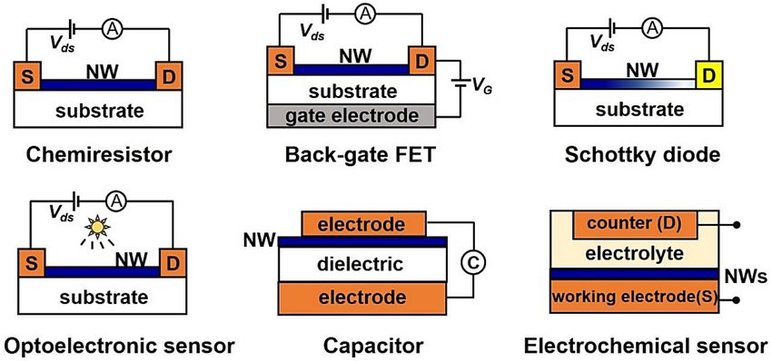
Sensors 2020, 20, 6781                                                                               8 of 41

literature, showing high selectivity and quantitative analytical information to target gases, pH, humidity,
glucose and DNA [27,36,49,140–146]. Capacitive-type sensors define the sensitivity using the change in
capacitance at a fixed voltage, and they are not generally applied to detecting inorganic gases [147,148].
SMO-NWs gas sensors based on these architectures are relatively less studied, either because of the
complexity in fabrication and measurement or low stability.
      Besides being arranged in a horizontal direction, recently, many nanowires have been developed
in a vertical architecture [149–153]. Multiple vertically aligned nanowires (VA-NWs) engage in the
sensing procedure, and thus the output signal is substantially increased. The VA-NWs also have
a higher exposed surface area than horizontal NWs because of the smaller contact area with the
substrates. Therefore, the VA-NWs can be used as versatile platforms for gas sensing applications.
Typically, Hung et al., reviewed the methods for on-chip growth of vertical SMO-NWs and their sensor
performance [84]. Other materials like silicon and GaN are also reported for VA-NWs gas sensors.
For instance, Ali et al., fabricated vertically aligned silicon nanowires (VA-Si NWs) by metal-assisted
chemical etching. The VA-Si NW gas sensor exhibited a response of 11.5–17.1 to 10–50 ppm H2
at 100 ◦ C.

2.4. Sensor Performance
      The performance of gas sensors is generally performed in a dynamic or static test instrument
with the temperature control module, gas flow controllers and data collection system. For practical
sensor products, important performance parameters include the sensitivity, the limit of detection (LoD),
the selectivity, the response and recovery time, the stability and the power consumption.
      Sensitivity and LoD are highly dependent on the physical form, structure and constituent of
the sensor material. For SMO-NWs with increased surface area, high sensitivity and low LoD are
extensively reported for various NW devices. In most cases, the sensitivity S is defined by the ratio of
electrical parameters (like sensor resistance) in air and in target gas. The LoD of the particular analyte
is related to the noise level of the sensor. According to the International Union of Pure and Applied
Chemistry (IUPAC), a reliable LoD can be calculated as a concentration of the analyte, which causes a
response 3 times higher than the noise level of the device [154,155]. Due to the negative impacts on
both environment and human life in many countries, the Environmental Protection Agency (EPA) has
regulated the limit of exposure to toxic and explosive gases, thus driving the continuous development
of high-sensitive gas sensors.
      Selectivity is defined by the ratios of the sensitivity of the target analyte to that of interfering
gases. It is widely known that selectivity is one of the biggest challenges for semiconductor sensors,
as their main sensing mechanism is based on the surface reaction of detectants with ionsorbed oxygen.
Gas sensors present responses to all oxidizing and reducing gases that contribute to the changed free
carrier concentration of the material. To date, most reported SMO-NW sensors obtained enhanced
selectivity from functionalization with metal nanoparticles or semiconducting elements that interact
selectively with a target gas or form heterojunctions with SMO-NWs [57,80,81,156–158]. Recently,
several methods have been developed to improve selectivity, such as pulsed temperature modulation,
microdiffusion, use of thermal gradients or cycled-temperature regime [159–163]. Selectivity toward
specific gases can also be achieved by optimizing the sensor architecture, designing sensor arrays and
training machine-learning-based classifiers (see details in Section 5.1) [30,37,145,157,164–174].
      Response time is determined by 90% of its final amplitude after analyte exposure, and the
recovery time is the time to decrease to 10% of the peak amplitude after removing the analyte.
In the reported literature, response time is governed by the factors of surface area, temperature and
catalysis [164,175–177]. Procedures for promoting sensor recovery mainly include resistive switching,
heat treatment and ultraviolet light exposure [178–183]. Moreover, long-term stability is also an
important parameter for reliable sensors and can be quantified by the response degradation of a
device over time. Many reported SMO-NW sensors remained unchanged over several months or
more [29,184,185]. The power consumption mainly originates from the electrical resistors for heating,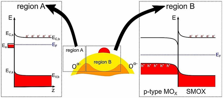
Sensors 2020, 20, 6781                                                                                     9 of 41

which is the main power-hungry part of the sensor device. In Section 4, we discuss the current sensor
technologies to optimize the power budget.

3. Structure-Performance Relationship
     Understanding the fundamental mechanism is an essential topic of gas sensor research. In the
1980s and early 1990s, significant contributions were made by Yamazoe et al., and Morrison,
describing the sensitization mechanism of metal/metal oxide-loaded SMO and the effects of size
on gas sensitivity [68,69]. Until today, these mechanisms are the basis for designing gas sensing
materials. However, the structure of sensing materials is becoming more complex and diversified,
and it is difficult to clearly describe the experimental findings using a single model. For SMO-NWs,
the reception and transduction of gas information are related to the changes of surface depletion layer
that can be influenced by the size and shape of NWs, the defect engineering, the doped or loaded
additives, and the contact geometry. This section intends to clarify the structure-function relationships
that are important for the knowledge-based design of high-performance gas sensors.

3.1. Size and Shape
     Size-related gas sensitivity can be explained by the classical D-L model [61], which compares
the NW diameter (D) and depth of surface charge layer (L). Large SMO-NWs offer a low surface
area-volume ratio, and only the geometrical surface can be affected by the gas molecules. As a result,
the changes of L are restricted to a small part of the sensing material, and the electrical transduction
can hardly be changed. When D is comparable to or less than 2L, the contribution of changes in surface
conductivity becomes prominent, as shown in Figure 5a. This phenomenon has been well observed in
many single crystalline NWs, which show enhanced gas sensitivity for a smaller diameter [186–188].

      Figure 5. Size and shape-related sensing model. (a) Schematic illustration of the relation between the
      NW diameter (D) and the depth of the surface charge layer (L). (b) Various classes of SMO-NWs with
      porous or branch-like structures.

     Another effective way to achieve high sensitivity is by using porous or branch-like structures,
as shown in Figure 5b. The increased surface area facilitates the interactions between the sensitive
material and the surrounding gases, which is the origin of enhanced sensor response. For example,
hollow SMO-NW (nanotube) has outer as well as inner surfaces. In 2011, Liu and coworkers synthesized
aligned ZnO nanotubes through combined electrospinning and sputtering techniques [189]. The sensor
response is 3.6 to 100 ppm H2 , much higher than that of ZnO film. Choi and Chang reported
the porous structured ZnO nanotube that showed improved H2 sensing response of 4.2 times of
porous ZnO film [190]. Other nanotube sensors like TiO2 , SnO2 , and ZnO/SnO2 composites were
also developed for detecting NO2 , butanone, ethanol, and other gases [140,189–196]. Branch-like
NWs can be classified as homogeneous or heterogeneous structure. ZnO nanocomb with the teeth
parts is considered as a homogeneous structure. Apart from the greater surface-to-volume ratio,
Pan et al., discovered that the teeth part of a ZnO nanocomb could serve as a “negative-potential gate”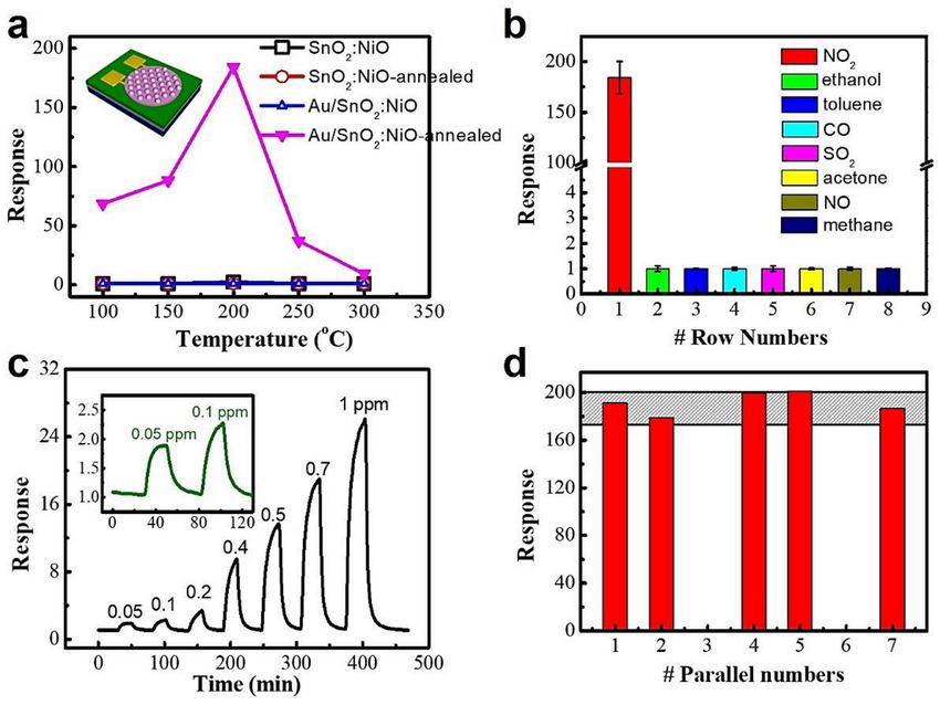
Sensors 2020, 20, 6781                                                                                   10 of 41

after accumulating electrons captured by surface adsorbed NO2 molecules, which also contributed to
the higher NO2 sensitivity [124,197]. Solution-based synthesis, especially the hydrothermal method,
has been considered a simple and powerful route for the preparation of hierarchical heterojunctions,
such as In2 O3 /ZnO core-shell NW and TiO2 /Sn3 O4 brush-like NW [60,81,95,158,198–200]. The overall
enhanced sensitivity of heterostructures has been generally reported to originate from the electrical
contributions of oxide-oxide heterojunction (p-n, p-p or n-n heterojunction) and the spillover effect.

3.2. Defect Engineering
      Gas-sensing properties of metal oxide materials are strongly related to the crystal defects of
electron donor and acceptor [201–207]. The micro-(µ) photoluminescence (PL) spectroscopy is an
effective technique to probe the crystal defects of individual nanostructures. In the case of pure ZnO
NWs, the deep level emission of µPL spectra originates from the donor level like oxygen vacancy (VO )
and zinc interstitial (Zni ), as well as acceptor levels like VZn , Oi , and OZn . The enhanced gas response
by defect engineering was mainly attributed to the rich electron donors for absorbing the largest
content of oxygen species. For example, Hong et al., reported that the sensitivity to NO2 was linearly
proportional to the PL intensity of VO in ZnO NWs [201]. Xue et al., reported the formation process of
rich VO and Zni defects by studying the ZnO nanodishes and achieved an excellent response of 49 to
100 ppm ethanol at 230 ◦ C [202]. The crystal facet-dependent gas sensing property proposed by Xu et
al., was also attributed to the large amount of VO and dangling bonds existing in ZnO nanosheets with
exposed crystal facet (0001) [203]. This mechanism has further been verified by our group, as shown in
Figure 6 [64]. According to the µPL subpeaks discriminated by Gaussian deconvolution, the single
ZnO NW with a diameter of ~110 nm has the maximum donors and thus displays the best sensor
response to acetone at 350 ◦ C (Figure 6a,b). This tendency is minimally affected by the junction in the
NW contact-based device (Figure 6c,d). We propose three models of sensing mechanism, including the
thinner single crystalline ZnO NW, the medium ZnO NW with many donor-related defects, and the
thicker ZnO NW with equal donor- and acceptor-related defects. The intrinsic excitation in the single
crystalline ZnO merely generates a few free electrons. While for thicker ZnO NW, many electrons are
consumed by the acceptor level. Therefore, only the medium ZnO NWs have enough free electrons to
adsorb more oxygen molecules, which contribute to the redox reactions with the target gas.

      Figure 6. Crystal-defect-dependent gas-sensing mechanism of the single ZnO NW sensors.
      (a) Responses to 5 ppm acetone versus operating temperature of the single ZnO NW with the diameter
      of ~110 nm. The inset is the corresponding SEM image of the gas sensor. (b) Relationship between
      acetone response of the ZnO NWs at 350 ◦ C (∆) and the donor level (O) and acceptor level () subpeak
      contents. (c) SEM image and schematic of an NW (~110 nm) contact-based device. (d) Responses to
      5 ppm acetone as a function of the diameter of the contacting ZnO NWs. Reprinted from reference [64]
      with permission from the American Chemical Society.
Sensors 2020, 20, 6781 11 of 41
3.3. Doped or Loaded Additives
Introducing additives in SMO-NWs is the most common way to achieve high sensitivity, selectivity,
and stability. The additives are loaded or doped with an additional compound, typically noble,
transition metals or other SMO. Doped SMO is the structure where additives are incorporated in the
lattice of SMO, as shown in Figure 7. Loaded SMO is a structure where the additive phase is separated
from SMO. Both of them can change the chemical and electrical sensing properties of SMO materials.
Figure 7. Different structures of SMO (blue) and added metal/metal oxide (red). For doped SMO,
additives are incorporated in the SMO lattice at the surface and/or in the bulk (figure (a)). For loaded
SMO, additives form a separate phase, which is smaller than the actual SMO grain and located at
the surface of SMO (figure (b)). Reprinted from reference [70] with permission from the American
Chemical Society.
The chemical contributions to sensor performance are mainly related to oxidation catalysis,
the sensing mechanism of which includes: (i) shift the reaction to the additive surface; (ii) activation of
lattice oxygen at the SMO−additive interface; and (iii) adsorption and activation of reactive species on the
additive surface and a subsequent spillover onto the SMO surface. As an example, the CuO-decorated
SnO2 NWs showed a high response of 3261—around 400 times that of pure SnO2 NW to 2 ppm
hydrogen sulfide (H2 S), because that CuO selectively react with H2 S, forming CuS [156]. A well-studied
example for activation of lattice oxygen is Pt-doped SnO2 [208–210]. Extended X-ray absorption fine
structure (EXAFS) and X-ray diffraction (XRD) analyses showed that Pt4+ could be easily incorporated
in the SnO2 lattice by replacing Sn4+ , leading to activation of lattice oxygen and an improved activation
of methane adsorption [209,211]. In the presence of Pt or Pd catalysts on the SMO-NWs, H2 binds,
dissociates, and spillover onto the SMO surface, thereby modifying the space charge layers of the
supporting SMO. Based on this sensing mechanism, high sensitive and selective H2 sensors have been
reported by many research groups [79,90,103,212–214].
The electrical contributions to sensor performance are related to the band bending by surface
states and the electronic coupling in the form of heterojunction between the additive and SMO material
(Figure 8). On one hand, the surface band bending occurs in the presence of charge located at the
SMO surface or SMO-additive interface. For n-type SMO, the electronic sensitization by an initial
upward band bending depends on the energy level and concentration of surface state, as shown in
region A of Figure 8 [70]. The relationship of the sensor signal and surface band bending is given by
S = exp[(eVs )/(kB T)], where e is the elementary charge, vs. is the surface potential, kB is the Boltzmann
constant, and T is the temperature. This initial surface band bending has a big impact on the conduction
mechanism and the concentration of surface oxygen species. Rebholz et al., showed the existence of
an intrinsic surface band bending for sol–gel-made SnO2 materials by simultaneous work function
measurements [211]. Moreover, the 1 at % Ni-loaded SnO2 was reported to have a huge intrinsic
surface band bending and an enhanced sensing performance in comparison to the undoped material.
On the other hand, the heterojunction caused by an alignment of two Fermi-levels can lead to a
higher upward band bending, as shown in the region B of Figure 8. This effect was observed in many
metal/SMO or p-n SMO heterostructures [58,74,158,215,216]. One example is the acetone sensing
with Rh-loaded WO3 [216]. When exposed to acetone, sensor resistance decreased. Meanwhile,Sensors 2020, 20, 6781 12 of 41
the heterojunction-induced space charge layer got thinner and thus less affected the WO3 oxygen
species, resulting in more W-O band in the infrared radiation (IR) spectroscopy. Our previous research
also demonstrated that the Fermi-level control sensitization is a powerful approach to rationally design
and optimize gas sensing materials [58]. Comprehensive reviews on this topic can also be found in the
literature [70,217].
Figure 8. Schematic illustration of the electric contributions. Region A corresponds to an unaffected
surface, where the space charge layer is controlled by the ionosorption of oxygen, forming a surface
state (Ea ). Region B corresponds to the heterojunction, where the space charge layer is controlled
by the Fermi-level of the loading. Reprinted from reference [70] with permission from the American
Chemical Society.
3.4. Contact Geometry
According to the device structure and working principle, NW contact geometry can be divided
into two types: inter-NW junction and Schottky junction, as shown in Figure 9 [71,72,218]. For single
NW devices, sensing mechanisms are dependent on the interaction between the analyte and individual
NW. While for NW networks, NW-NW junction-type of contacts exist, which are extensively
investigated for their ability to control the barrier height and achieve the on-chip fabrication of NW gas
sensors [73,93,171,219–222]. According to the semiconductor nature of materials, NW-NW junctions
include n-n, p-p and n-p inter-junctions, as shown in Figure 9a.
Figure 9. Schematic of NW contact-based sensing mechanisms. (a) The schematic of the gas sensing
mechanism of NW-NW junctions based on SnO2 /ZnO hierarchical nanostructures. Reprinted from
reference [72] with permission from Elsevier B. V. (b) The structure of Schottky-contacted NW sensor,
and the change of Schottky barrier height (SBH) and depletion region under the external stimulation.
Reprinted from reference [218] with permission from Wiley-VCH.Sensors 2020, 20, 6781 13 of 41
Numerous reports available in the literature demonstrate that NW-NW junctions facilitate the
low concentration gas detection, as the conduction path involves tunneling through the depletion or
accumulation layer. Park et al., reported x2 the junction-tuned SnO2 NW sensors by changing the
spacing of patterned-interdigital electrodes (PIEs) [221]. The narrower spacing of PIEs led to a high
density of NW-NW junctions, and thus superior properties for NO2 sensing. Cui et al., fabricated highly
sensitive H2 S sensors based on Cu2 O/Co3 O4 p-p heterojunction and achieved a sub-ppm LoD [215].
The difference between n-n, p-p and n-p junctions was studied based on the air-bridged ZnO/CuO
NWs [171]. In ZnO/ZnO n-n junction and CuO/CuO p-p junction, the electron or hole must pass
the overlapping NWs over the barrier height. In ZnO/CuO n-p junction devices, electrons flow
over the build-in potential, whereas the less effective transduction for p-type CuO decreases the
sensitivities of the gases. The interfacial potential energy barrier (V) related resistance (R) can be
defined as R = R0 exp[(eV)/(kB T)]. Apart from this energy barrier, some papers proposed that the
inter-NW junction can also narrow the charge conductance channel via the formation of the depletion
region, and thus make the resulting depletion region boundary more sensitive than that of the depletion
region created directly by the adsorption and desorption of oxygen [223–225]. The origin and sensing
mechanism of the Schottky junction in Figure 9b have been discussed in Section 2.3. A comprehensive
review of the topic of Schottky-contacted NW sensors can also be found in the recent literature [71,134].
4. Toward Low Power Consumption
Power consumption is a tough problem both for the application of SMO sensors in IoT programs
and the integration of metal oxides into flexible and/or wearable sensors. Strategies for ultra-low
power consumption are concluded as thermal isolation, self-heating and developing room-temperature
sensors, which work either by decreasing the sensing area or by reducing the working temperature.
4.1. Thermal Isolation by MEMS Techniques
Most of the reported SMO sensors are based on the ceramic tubes in Figure 10a [226–232].
The sensors are made by coating alumina tube with the solution based SMO paste to form a thin
sensing layer. The heating wire of Ni-Cr is inserted in the tube to indirectly heat the sensor. A pair
of gold electrodes are installed by twining gold wires on the tube to measure the electrical signal.
The power consumption of this type of gas sensor is more than 1 W. Some research tried to decrease
the size of ceramic substrates and fabricated SMO sensors on alumina plates (Figure 10b) [233].
The sensing materials are also made into a slurry and then deposited onto the alumina plates with a
screen-printed platinum heater. This method helps to reduce the power consumption to hundreds of
milliwatts. However, the low manufacturing efficiency, lack of integration capability, together with
large sensor-to-sensor variations, limits their practical application and marketing.
The emergence of MEMS techniques has opened up new options for the realization of low energy
dissipation, device miniaturization, large-scale device production. The study of MEMS gas sensors
started in the early 1990s. The scheme, structure and photo of one first sensor based on this approach
were first presented by Chaudret et al., as shown in Figure 10c [234]. The hot sensing area is located
at a small scale by etching of silicon from the back sides of the wafer, and in this way, the thermal
inertia is drastically reduced. All this period since 90th was dedicated to optimize MEMS layout,
to choose optimal materials for the heater and for the insulating layer, and to improve the adhesion
between materials at high temperature. Current mass-production silicon MEMS technology has already
permitted the effective heating of microhotplates at temperatures lower than approximately 400–450 ◦ C
with the power consumption less than 50 mW [77,235–238]. However, the integration of sensing layers
with the MEMS microhotplates is still a technological challenge.
Up to now, several novel MEMS gas sensors have been reported, which can be divided into three
categories. In the first case, the slurry of chemically synthesized nanomaterials is drop-coated or printed
onto the small and suspending active area of MEMS microhotplates [75,122,237–241]. For example,
Andio et al., have demonstrated a high-performance CO gas sensor with SnO2 nanoparticle-laden inkSensors 2020, 20, 6781 14 of 41
deposited on a microhotplate via inkjet printing [235]. Li et al., reported the efficient hierarchical mixed
Pd/SnO2 porous composites deposited on the microheaters using the microdispensing method and
achieved high sensing performance towards ethanol at low power consumption [238]. These kinds
of methods are particularly difficult and complicated with low yield, low efficiency and large
sample-to-sample deviation. For the second category, the site-specific growth of SMO-NWs on
microheaters can directly achieve on-chip integration. Hrachowina et al., proved this concept
by growing SnO2 , WO3 , and Ge NWs on the same microheater chip using CVD techniques [56].
The discrimination between CO, NO2 , and different levels of relative humidity was obtained by
the obtained high-performance gas sensors and the principal component analysis (PCA) method.
Nevertheless, the microheater substrates may degrade and even be destroyed under high-temperature
conditions of the NWs growth. In the third category, sensing films are deposited by the typical MEMS
or MEMS compatible techniques, such as sputtering, evaporation, chemical vapor deposition (CVD)
and self-assembly [233,236,242–245]. Additional thermal oxidation, annealing or acid treatments are
subsequently needed to modify the as-deposited compact and amorphous structure. For example,
Kang et al. reported a sputtered SnO2 thin film-based micro gas sensor, which showed a response
of 6–25 ppm toluene at 450 ◦ C [236]. Our group has designed a MEMS compatible gas sensor with
sputtered SnO2 :NiO thin film deposited on self-assembled Au nanoparticle arrays and obtained a
high response of ~185 to 5 ppm NO2 , as shown in Figure 11 [58]. These Au/SnO2 :NiO sensors exhibit
a high response of ~185 to 5 ppm NO2 , low LoD of 50 ppb, high selectivity, good stability and also
sensor deviation of less than 15%. Moreover, we also achieved activating the sputtered SnO2 :NiO
thin film by fabricating cross-linked network structures and by Pd-doping for highly sensitive ethanol
detection [29,246]. This type of MEMS sensor shows promising potency in the production of wafer-scale
gas sensors with low sensor-to-sensor deviation. Even so, many efforts are still highly desirable towards
more simple strategies to control sensing film parameters, including the composition, structure and
doping state.
Figure 10. SMO sensors based on various substrates. (a) Schematic diagram of the sensor based
on the ceramic tube substrate. Reprinted from reference [226] with permission from Elsevier B. V.
(b) Schematic and photo of the sensor based on alumina plate. Reprinted with permission from [233].
(c,d) Scheme and photo of the microhotplate fabricated using silicon micro electro mechanical system
(MEMS) techniques. The a–g in the figure (c) corresponds to the metal line for the sensing layer,
dielectric layer, passivation layer, heater metal, polysilicon heater, silicon frame, and dielectric membrane,
respectively. Reprinted with permission from [234].Sensors 2020, 20, 6781 15 of 41
Figure 11. MEMS compatible NO2 sensors based on sputtered SnO2 : NiO thin films on self-assembled
Au nanoparticle arrays. (a) Response to 5 ppm NO2 vs. operating temperature of the SnO2 : NiO, SnO2 :
NiO/Au and Au/SnO2 :NiO thin-film sensors. Inset: Schematic diagram of the sensor. (b) The selectivity
of the Au/SnO2 : NiO sensor. (c) The dynamic sensing response measurements of the Au/SnO2 : NiO
sensor at 200 ◦ C. The inset figure shows the measured LoD is 50 ppb. (d) Comparison of responses of the
Au/SnO2 : NiO sensors with different numbers of devices in parallel to 5 ppm NO2 at 200 ◦ C. The gray
rectangle shows that the device deviation is less than 15%. Reprinted with permission from [58].
4.2. Self-Heating
The self-heating operation is to make use of the local high temperature created by the Joule
dissipation during the electrical probing. This strategy is typically proposed for chemiresistor based
on monocrystalline NWs [45,59,80–82,84,247–253]. With the bias current applied in conductometric
measurements, NWs heat up to relatively high temperatures by the Joule effect and can even
melt. The tiny mass of NW allows a remarkable increase in temperature, even when only a small
bias voltage is applied. According to the reported self-heated devices based on single SnO2 NW,
working temperatures in the range of 100–400 ◦ C can be achieved with the power consumptions below
100 µW [59,82,254,255]. In addition to the ultra-low working power, the self-heating approach has three
other advantages: (1) making the device architectures more simple by removing the need for external
heaters, (2) improving the sensor response with fast thermal response times, and (3) allowing good sensing
performances on flexible/wearable substrates. Typically, Meng et al. utilized a pulsed self-Joule-heating of
suspended SnO2 NW, which enabled not only the gigantic reduction of energy consumption down to
102 pJ/s but also enhancement of the sensitivity for electrical sensing of NO2 (100 ppb) [256].
However, fabricating efficient self-heating sensor devices for practical application is still distant.
First, the calibration and control of the power–temperature characteristics of NW devices are extremely
difficult. Traditional techniques based on the thermal equilibrium between sample and probe are not
suitable for NW sensors due to the huge perturbations in the temperature during the measurement.
Only estimated values of the temperature can be quickly obtained by indirectly comparing the resistance
or gas response in self-heating and in external heating operation. The thermal losses by conduction
with the substrates, the contact pads, and the surrounding gas also limit the accuracy in controlling
the actual temperature reaching the self-heating mode [257–262]. Second, the dimension, shape and
constitute of NWs, have a strong impact on the thermal distribution, electrical properties, as well
as thermal conductivity. As a reference, the temperature is inversely proportional to the square of
the radius of NW [82]. Thus, the synthesis of monodispersedly sized SMO-NWs is crucial for the
large-scale production of reliable self-heating sensors. Third, there exists a risk of damaging the sensorSensors 2020, 20, 6781 16 of 41
due to the burning of the NW at a high input power. While for low input power, the conductivity
range of NW sensors requires more complex and expensive electronics. Multiple-wire configurations
like aligned NWs and NW networks may help to handle this contradiction and also facilitate sensor
integration [73,157,189,263,264]. The recent study of self-heated SMO-NW sensor is reported by Ngoc
et al., who present an effective SnO2 NW sensor for reducing gases by using the Joule heating effect
at inter-NW junctions [59]. The sensor’s power consumption is around 4 mW, already meeting the
requirement for application in mobile phones.
4.3. Room-Temperature Sensing
Room-temperature sensing has been proposed toward zero power consumption. Nitrogen oxide
and hydrogen interaction with SMO nanostructures at room temperature are the most studied areas.
The Zhou group reported the detection of NO2 down to ppb levels using single and multiple In2 O3
NW FET sensors operating at room temperature [265]. Fan et al., also reported a ZnO NW FET
sensor, showing highly sensitive properties toward NO2 [266]. A number of articles present that the
Pd/SMO or Pt/SMO nanostructures possess the unique sensing mechanism of forming hydride and
thus exhibit highly selective H2 detection [79,103,213,214]. Due to the slow interaction dynamics,
the response speed for room-temperature sensing was relatively low, and extra electro-desorption or
optical-desorption was explored to speed up the recovery process and to achieve the complete recovery
of measured electronic parameters [178–183]. Moreover, the electric field-assisted and light-activated
absorption/desorption of target gases were also used to improve the sensor sensitivity and selectivity.
Recently, Zhou et al., have prepared a ZnO NW network sensor and studied the room-temperature
sensing performance toward trace NO2 under ultraviolet (UV) illumination [267]. With UV exposure,
the adsorbed oxygen ions were weakly bonded on the ZnO surface, facilitating the reversible response
of 157 to 50 ppb NO2 at room temperature. Visible light-activated excellent NO2 sensors based on
ZnO/g-C3 N4 composites are reported, showing the LoD of 38 ppb [268].
Other effective strategies to lower the working temperature are surface modification, additive doping,
or fabrication of heterostructures [269–273]. Oleg et al., have reported the sensor devices based on
multiple networked Au/ZnO NWs, showing a high response of 40 to 100 ppm H2 and a low theoretical
LoD below 1 ppm [263]. The high gas response was explained based on a gas sensing mechanism,
which includes the modulation of multiple potential barriers between the NWs and the role of noble metal
nanoclusters. Pham et al. studied the VLS catalytic growth of the biaxial p-SnO/n-ZnO heterostructured
NWs and achieved a good sensing performance to ppb-level NO2 at room temperature without light
illumination [274]. This p-SnO/n-ZnO device also showed a low LoD of 50 ppb under various relative
humidity. Shen et al., reported interesting results for room-temperature sensing performances of
mesoporous In2 O3 nanorod arrays on a porous ceramic substrate for ppb-level NO2 detection [37].
The response value to 800 ppb NO2 was 14.9 with a short response time of 14 s. Non-stoichiometric
SMO materials like W18 O49 NW networks showed highly enhanced ammonia sensing properties at
room temperature due to the large amounts of oxygen vacancies that facilitate the chemisorption of
oxygen at a low temperature [275].
Nowadays, the on-chip fabrication of optoelectronic chemiresistors is attractive for room-
temperature monitoring due to their highly enhanced selectivity and easy implementation with
micro light-emitting diodes (µLEDs) or optical fiber technology [32,78,127,276–278]. Cho et al.,
designed the monolithic photoactivated gas sensor based on the integration of ZnO NWs on µLEDs,
as shown in Figure 12a,b [128]. The sensor showed excellent NO2 sensitivity (∆R/R0 = 605% to 1 ppm
NO2 ) at the operating power of 184 µW (Figure 12a,b). Chen et al., also reported the mesostructured
ZnO NW photoelectronic formaldehyde sensors that exhibited an LoD of as low as 5 ppb and a response
of 1223% (at 10 ppm) [278]. Microlight plate configuration allows for the device miniaturization
and the power consumption as low as 30 µW. A comprehensive review on UV-LED photo-activated
chemical gas sensors was presented by Espid and Taghipour, illustrating the recent progress in thisYou can also read