Silicon-organic hybrid photonics: an overview of recent advances, electro-optical effects and CMOS integration concepts - IHP Microelectronics
←
→
Page content transcription
If your browser does not render page correctly, please read the page content below
TOPICAL REVIEW • OPEN ACCESS

Silicon-organic hybrid photonics: an overview of recent advances,
electro-optical effects and CMOS integration concepts
To cite this article: Patrick Steglich et al 2021 J. Phys. Photonics 3 022009

View the article online for updates and enhancements.

                              This content was downloaded from IP address 194.95.141.200 on 09/04/2021 at 09:16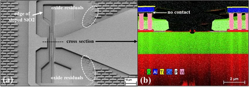
J. Phys. Photonics 3 (2021) 022009 https://doi.org/10.1088/2515-7647/abd7cf
Journal of Physics: Photonics
TOPICAL REVIEW
Silicon-organic hybrid photonics: an overview of recent advances,
OPEN ACCESS
electro-optical effects and CMOS integration concepts
RECEIVED
29 October 2019 Patrick Steglich1,2,∗, Christian Mai1, Claus Villringer2, Birgit Dietzel2, Siegfried Bondarenko2,
REVISED Viachaslau Ksianzou2, Francesco Villasmunta1,2,3, Christoph Zesch2, Silvio Pulwer2, Martin Burger2,
27 August 2020
Joachim Bauer2, Friedhelm Heinrich2, Sigurd Schrader2, Francesco Vitale3, Fabio De Matteis3,
ACCEPTED FOR PUBLICATION
3 January 2021 Paolo Prosposito3, Mauro Casalboni3 and Andreas Mai1,2
1
PUBLISHED IHP—Leibniz-Institut für innovative Mikroelektronik, Im Technologiepark 25, D-15236 Frankfurt (Oder), Germany
2 April 2021 2
Technical University of Applied Sciences Wildau, Hochschulring 1, D-15745 Wildau, Germany
3
University of Rome ‘Tor Vergata’, Department of Industrial Engineering, I-00133 Rome, Italy
∗
Original Content from Author to whom any correspondence should be addressed.
this work may be used
under the terms of the E-mail: steglich@ihp-microelectronics.com
Creative Commons
Attribution 4.0 licence. Keywords: silicon photonics, silicon-organic hybrid, electro-optical effects, Pockels effect, Kerr effect, slot waveguide,
Any further distribution
photonic integrated circuits
of this work must
maintain attribution to
the author(s) and the title
of the work, journal Abstract
citation and DOI.
In recent decades, much research effort has been invested in the development of photonic
integrated circuits, and silicon-on-insulator technology has been established as a reliable platform
for highly scalable silicon-based electro-optical modulators. However, the performance of such
devices is restricted by the inherent material properties of silicon. An approach to overcoming
these deficiencies is to integrate organic materials with exceptionally high optical nonlinearities
into a silicon-on-insulator photonic platform. Silicon–organic hybrid photonics has been shown to
overcome the drawbacks of silicon-based modulators in terms of operating speed, bandwidth, and
energy consumption. This work reviews recent advances in silicon–organic hybrid photonics and
covers the latest improvements to single components and device concepts. Special emphasis is
given to the in-device performance of novel electro-optical polymers and the use of different
electro-optical effects, such as the linear and quadratic electro-optical effect, as well as the
electric-field-induced linear electro-optical effect. Finally, the inherent challenges of implementing
non-linear optical polymers on a silicon photonic platform are discussed and a perspective for
future directions is given.
1. Introduction
With the fast evolution of data traffic in worldwide communication networks, the microelectronic industry
requires significant advancements in chip-integrated communication systems. Photonic integrated circuits
based on silicon-on-insulator (SOI) technology have attracted increasing research interest and play a major
role in this development [1]. SOI technology provides the ability to fabricate silicon photonic devices
together with electronic devices on a single chip [2–5]. The integration of photonic devices on SOI
substrates has reached industrial standards due to substantial research investment [6–8]. Today,
complementary-metal-oxide-semiconductor (CMOS) fabrication methods are used to produce photonic
integrated circuits at the wafer level. Therefore, photonic integrated circuits will play an omnipresent role,
impacting such areas as high-speed communications for mobile devices, optical communication within
computers, and data centers, and within sensor systems for medical applications [7, 9–14]. Ongoing research
aims to increase data rates with high signal quality while reducing the associated energy consumption [15].
In general, electro-optical (EO) signal modulation is the key function in many types of
telecommunication devices. In the case of silicon-based systems, one can distinguish between two major
groups of EO modulators, classified by their material systems. The first relies on the plasma dispersion effect
of silicon itself [15], while the second relies on the non-linear properties of a hybrid integrated material on
© 2021 The Author(s). Published by IOP Publishing Ltd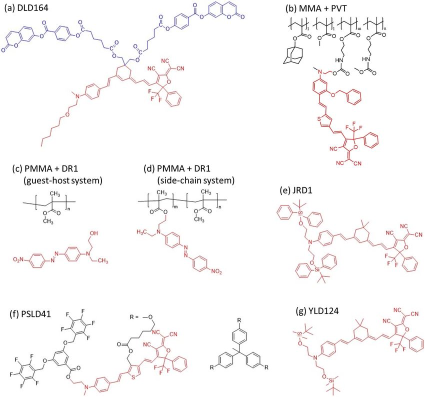
J. Phys. Photonics 3 (2021) 022009                                                                    P Steglich et al

silicon that provides a strong Pockels (linear EO) or Kerr (quadratic EO) effect [16]. Silicon-based
modulators consist of silicon waveguides, which are typically doped in such a way that they form either a
pn-diode or a pin-diode. By applying a voltage to the waveguide, the optical properties of the waveguide are
changed. EO modulators employ this effect to modulate light in dependence on an applied driver voltage.
Fundamental speed limitations are related to carrier transport mechanisms (injection and removal of
carriers). Therefore, parametric processes are impaired by nonparametric processes such as two-photon
absorption, which become the main limiting factor. Moreover, silicon suffers from a linear EO effect and, as a
consequence, detrimental coupling of the amplitude and phase of the guided optical wave [17]. This makes
higher modulation formats challenging to realize and usually leads to relatively high energy consumption.
Therefore, recent research has focused on the hybrid integration of a second material system, e.g. III–V
compounds [18], lithium niobate thin films [19], barium titanate [20], phase-change materials [21], or
organic EO materials [22]. The latter is within the scope of this review.
     Silicon–organic hybrid (SOH) photonics, i.e. the combination of silicon photonics with functionally
optimized organic EO materials, offers an approach to solving these problems [23, 24]. SOH photonics is a
viable extension of SOI technology. In recent years, there has been an increasing interest in SOH photonics,
mainly supported by two developments. First, increasingly rapid advances in the field of organic EO
materials have been accomplished in the past thirty years, leading to remarkable non-linear optical
properties [25, 26]. Second, an innovative silicon waveguide structure, known as slot waveguide, was
introduced in 2004 [27, 28]. This waveguide structure fits very well with the use of photonics SOI platforms.
     Organic materials exhibit off-resonant EO properties allowing for the manipulation of the amplitude and
phase of the optical carrier wave independently of each other using an interferometric configuration. Thus,
they enable the realization of higher modulation formats and high-bit-rate data transmission. Moreover,
such SOH modulators are extremely energy-efficient and can overcome the limitations of current
silicon-based modulators [29] because the electric field is sufficient to change the refractive index without
carrier injection. This minimizes carrier transport and reduces the device’s capacitance, a major cause of the
relatively high energy consumption of currently established EO modulators.
     Potential applications that can be enabled by SOH photonics are: high-speed modulators with ultra-low
energy-consumption [29], frequency combs featuring flat-topped spectra [30, 31], tunable optical filters
exhibiting ultra-high wavelength tuning [32], non-linear optical devices for frequency doubling [33], and
laser sources [34]. The nonlinear optical properties of organic materials [35], and the simultaneous use of
linear and quadratic EO effects [36] also offer perspectives for novel device concepts for programmable
photonics [37].
     This paper reviews the recent advances in SOH photonics based on SOI technology with a special
emphasis on the in-device performance of EO polymers, and reports on the latest developments of SOH
key-components such as slot waveguides and strip-to-slot mode converters. It is mainly devoted to the
following aspects: (a) advances in SOH device concepts and the operating principles of SOH devices,
(b) in-device performance of EO polymers, and (c) an overview of CMOS integration concepts.

2. Advances in SOH device concepts

2.1. Slot waveguide
The concept of the slot waveguide plays a key role in SOH photonics. Almeida et al [27] proposed this novel
waveguide structure in 2004 and Xu et al [28] provided the first experimental proof in the same year.
A SOI slot waveguide consists of two silicon rails separated by a sub-wavelength distance. A comprehensive
study of SOI slot waveguide structures can be found in [38]. Figure 1 shows a comparison between the
optical field distribution in a common strip waveguide and that of a slot waveguide. As can be seen from this
figure, the light is mainly confined in the high-index silicon strip waveguide, while for slot waveguides the
light is mainly in the cladding material between the two silicon rails, making an efficient interaction between
the guided light and the non-linear optical cladding material feasible.
    Electrical connections to the two walls of the slot waveguide are necessary to perform modulation of the
light, meaning that doped silicon has to be used, as illustrated in figure 2, where optical 2(a) and electrical
2(b) field distributions are depicted.
    The main advantage of slot waveguides lies in the previously mentioned high field confinement inside the
slot, which leads to a strong interaction between the guided light and the interposed cladding material (EO
polymer). In recent years, there has been an increasing amount of literature concerning the field confinement
in slot waveguides aimed at improving the waveguide geometry for EO applications [39–43]. Several studies
have revealed that it is not just the slot width, s, that influences the field confinement but also the rail width,
w. The optimized field-confinement factor inside the slot of a vertical silicon slot waveguide fabricated using

                                              2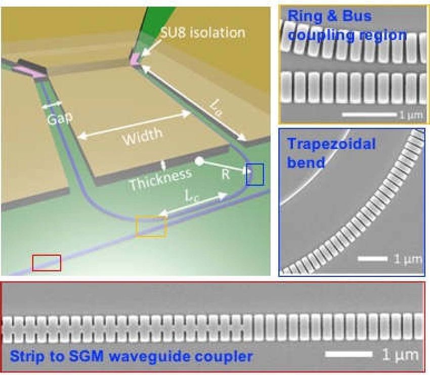
J. Phys. Photonics 3 (2021) 022009                                                                                            P Steglich et al

   Figure 1. Numerical simulation of the normalized E-field intensity |Ex |2 + |Ey |2 + |Ez |2 for the quasi-transversal electric (TE) and
   quasi-transversal magnetic (TM) modes of SOI strip and slot waveguides: (a) strip waveguide (TE mode); (b) strip waveguide
   (TM mode); (c) slot waveguide (TE mode); (d) slot waveguide (TM mode). Adopted from [38].

   Figure 2. (a) Normalized optical field distribution of the quasi-TE eigenmode of an SOH slot waveguide with silicon strip loads in
   an SOI technology and (b) normalized electric field distribution (E). The largest overlap between the optical and electrical fields is
   achieved within the slot region. Therefore, EO effects outside the slot region are negligible, and hence, the field confinement
   factor in the slot region should be taken into account to avoid an overestimation of the refractive index change. © 2018 IEEE.
   Reprinted, with permission, from [65].

SOI technology is about 0.2; i.e. only ≈20% of the guided light interacts with the EO polymer and the
applied electric field. However, the relatively large overlap between the electric and optical fields leads to an
efficient phase shift of the guided light. A more comprehensive study of the field confinement factor of SOI
slot waveguides can be found in [44].
     In recent years, slotted photonic crystal waveguides have been demonstrated to be appropriate candidates
for use in SOH photonics [45–50]. Slotted photonic crystals allow for slow light propagation and strong field
confinement, enabling efficient EO modulation [51, 52], and can form a resonator by employing different
photonic crystal dimensions along the length of a slot waveguide [53, 54], as shown in figure 3. The resonator
is defined by the cavity region (PhC1) and the reflector (PhC2). An injector section (PhC3) between PhC2
and the slot waveguide is implemented for low-loss light coupling.
     The main drawback of slot waveguides is the relatively large optical loss caused by sidewall roughness.
Slot waveguides typically have propagation losses of around 4 dB mm−1 [55], while slotted photonic crystal
waveguides show even higher losses of 15 dB mm−1 for 1D photonic crystal slot waveguides [56] and
20 dB mm−1 for 2D photonic crystal slot waveguides [57]. In the case of slotted photonic crystal waveguides,
a record low propagation loss of 5.1 dB mm−1 has been demonstrated by introducing the photonic crystal
structure inside the slot [58]. However, a promising approach for tackling the general issue of high
propagation loss in slot waveguides is to cover the slot waveguide with an atomic layer of a thin dielectric
film, e.g. amorphous titanium dioxide (TiO2 ), thereby reducing the propagation loss to 7 dB cm−1 [59–62].
However, the additional atomic layer can also be used to reduce the slot width, s. For example, a slot width of
about 34 nm was demonstrated using atomic layer deposition of Al2 O3 [63]. Additionally, gold can
subsequently be deposited, to further reduce the gap to 15 nm, which eventually creates a plasmonic
structure. Although the atomic layer deposition of TiO2 or Al2 O3 reduces the propagation loss and slot
width, it is associated with additional and cost-inefficient production steps, which makes it rather
unattractive from a commercial point of view. The most recent advances in waveguide production, however,
have led to the reduction of losses to as little as 3.7 dB cm−1 without atomic layer deposition [64]. In this

                                                         3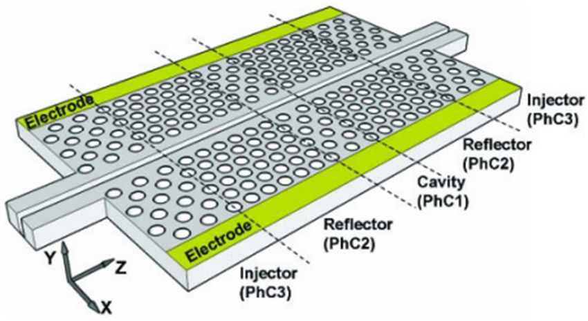
J. Phys. Photonics 3 (2021) 022009                                                                                     P Steglich et al

   Figure 3. A slotted photonic crystal (PhC) waveguide structure, forming a resonator for EO modulators. Adopted from [53],
   © 2009 Optical Society of America.

   Figure 4. (a) Direct mode-coupler strip-to-slot mode converter. (b) Gradual waveguide taper strip-to-slot mode converter.
   Adopted from [71].

case, to reduce sidewall roughness, a tetramethylammonium hydroxide-based anisotropic wet-etching
technique was applied following waveguide fabrication using e-beam lithography and a dry-etch process.

2.2. Strip-to-slot mode converter
To minimize the optical losses of a device, it is convenient to make the region of the waveguide containing the
slot as short as possible. This implies that particular attention must be paid to strip-to-slot mode conversion,
which plays a vital role in SOH photonics. Strip-to-slot mode converters are designed to achieve a smooth
transition between strip and slot waveguides. An efficient strip-to-slot waveguide transition is needed to
exploit the advantages of both strip and slot waveguides, and to combine them in a single device or circuit.
Strip-to-slot mode converters can be achieved by either implementing a slowly varying waveguide taper
[66–68] or a direct mode coupler [69, 70].
    Direct strip-to-slot mode converters permit a highly compact solution and have been demonstrated to
offer efficient modal coupling. Figure 4(a) shows a numerical simulation of a simple direct mode converter.
Typical loss values of about 0.91 dB can be achieved for such a direct strip-to-slot mode converter, as
experimentally shown in [70]. Since the conversion efficiency is only adequate at narrow slot widths, i.e.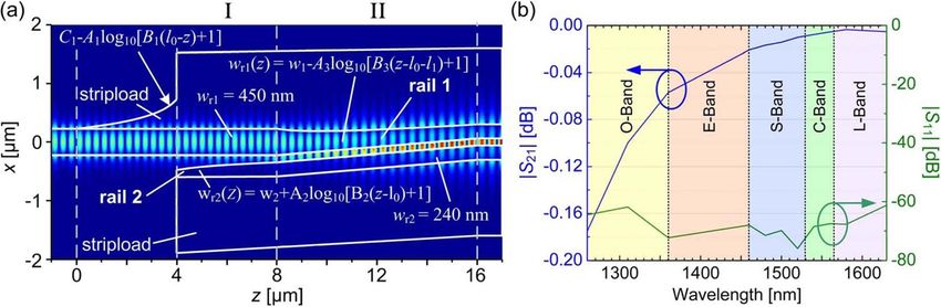
J. Phys. Photonics 3 (2021) 022009                                                                                         P Steglich et al

   Figure 5. (a) Electric field distribution of a logarithmic slowly varying waveguide taper. (b) Simulated S-parameters of a converter
   as a function of wavelength. S21 indicates the transmission and S11 the reflection at each mode converter. Adopted from [66].

2016, Deng et al [69] expanded this concept to obtain a polarization-insensitive direct mode converter.
Measured conversion efficiencies of 95.9% for TE0 and 96.6% for TM 0 were achieved. More recently, another
innovative direct mode converter was presented by Mere et al [73]. Their mode converter consisted of a
balanced 50/50 power splitter and a tunable phase-matched taper combiner forming a slot waveguide. They
experimentally demonstrated a coupling efficiency of 99%.
     One drawback of direct mode converters is that they are not usable in EO phase shifters because the
silicon rails are connected to each other, and they form an electric conductor, making electric field
generation impossible. In this case, slowly varying waveguide tapers are preferred for EO modulators. A
numerical simulation of such a mode converter is shown in figure 4(b). As can be seen from this figure, the
upper silicon rail is separated from the lower one. Consequently, this type of mode converter forms a
capacitor when a voltage is applied to the silicon rails. In 2011, Yang Liu et al published a paper in which they
described a mode converter based on a slowly varying waveguide taper with losses of around 0.81 dB [67]. In
2013, Palmer et al investigated the same type of mode converter and achieved record low losses of about
0.02 dB and negligible reflections between 1480 and 1580 nm [66]. This was achieved by the use of a
logarithmic slowly varying waveguide taper instead of a linear one, as shown in figure 5.

2.3. Mach–Zehnder interferometer
A schematic representation of a SOH Mach–Zehnder interferometer is shown in figure 6. Mach–Zehnder
interferometers are composed of either one Y-splitter and one Y-combiner, or of a 1 × 2 multimode
interference (MMI) splitter and a 2 × 1 MMI combiner. The slot waveguide is electrically connected, so that a
ground–signal–ground (GSG) coplanar traveling-wave electrode configuration with a 50 ohm termination is
realized for push-pull operation. The slot waveguide is infiltrated with an EO polymer and serves as an active
phase shifter. In this way, ultra-compact SOH Mach–Zehnder modulators with slot waveguide lengths as low
as 500 µm were demonstrated [74]. However, typical slot waveguide lengths range from 1 to 2 mm.
    SOH Mach–Zehnder modulators benefit from the off-resonant Pockels effect, making higher modulation
formats feasible. In particular, IQ-modulators have been demonstrated by combining two SOH
Mach–Zehnder modulators, as schematically shown in figure 7. Here, I stands for the in-phase and Q for the
quadrature component. During the last decade, several SOH Mach–Zehnder modulators have been
demonstrated to operate at 10 Gbit s−1 [29], 12.5 Gbit s−1 [75], 40 Gbit s−1 [23], 84 Gbit s−1 [76],
100 Gbit s−1 [77], 112 Gbit s−1 [78] and 120 Gbit s−1 [79] and advanced modulation formats such as
16QAM (quadrature amplitude modulation) [75] as well as OOK (on–off keying), BPSK (binary phase-shift
keying), 8-ASK (amplitude-shift keying with 8-binary symbols) [80] and PAM4 (four-level pulse-amplitude
modulation) [77, 79] signals have also been demonstrated. These results suggest that SOH phase shifters
enable higher-order modulation formats without compromising on signal quality, and therefore have high
potentiality in the field of communication systems.
    The voltage-length product is a figure of merit that can be used to compare state-of-the-art phase shifters
based on SOH slot waveguides with depletion-type phase shifters. It is often used in the literature to
characterize the effectiveness of phase-shifters. It is defined as the voltage Uπ needed to induce a phase shift
of π multiplied by the phase shifter’s length, which is just the slot waveguide’s length Lslot [81].
    There are several publications targeting low voltage-length products by the use of Mach–Zehnder
interferometers [77, 79, 82–84]. In 2014, Lauermann et al [85] experimentally showed a SOH Mach–Zehnder
modulator with a voltage–length product of only 0.53 V mm and an energy consumption of less than
19 fJ bit−1 .

                                                        5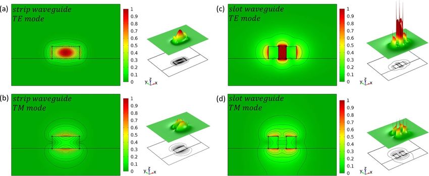
J. Phys. Photonics 3 (2021) 022009                                                                                        P Steglich et al

   Figure 6. (a) Schematic of a Mach–Zehnder SOH modulator. The black lines represent SOI strip waveguides. The phase-shifter
   sections are based on slot waveguides having a slot width s. The traveling-wave electrodes are configured as ground–signal–
   ground (GSG) and carry the electrical modulation signal. (b) Schematic of the cross-section along the lines A and B illustrated in
   (a). The slot waveguide is connected to metal electrodes by doped silicon striploads and tungsten vias.

   Figure 7. Schematic of a SOH in-phase quadrature (IQ) modulator. The IQ modulator consists of two nested Mach–Zehnder
   modulators and one half-wave phase shifter (π/2).

2.4. Ring resonators
High-performance EO modulators based on SOH photonics have mostly been demonstrated using
Mach–Zehnder interferometers. On the one hand, these modulators are appropriate candidates for the
generation of higher-order modulation formats, but, on the other hand, their large footprint represents a
substantial limitation, resulting in a large areal consumption on the chip and a high insertion loss. To
overcome these restrictions, a different modulator geometry has been proposed, namely optical ring
resonators, as shown in figure 8(a). Indeed, ring resonators are applicable as EO modulators as well as for
tunable filters and switches. They are significantly smaller, which is of great benefit in achieving high
integration densities, low optical losses, and low energy consumption.
    Only a few SOH ring resonator modulators have been described that used SOI technology . The main
reason for this is that SOI slot waveguides suffer from relatively high losses. This is mainly caused by sidewall
roughness [87]. As a consequence, slot waveguide resonators such as micro-ring resonators typically have
small optical quality factors (Q-factors) [88–90]. One possible approach to tackle this problem is to reduce
propagation losses in slot waveguides by atomic layer deposition, as described in the previous section.
However, a slot waveguide ring resonator modulator having a 6 dB bandwidth of 1 GHz, a device tunability of
12.7 pm V−1 , and a Q-factor of 5000 was demonstrated in 2011 [88]. Furthermore, a double-slot waveguide
ring resonator covered by liquid crystal was proposed and theoretically analyzed to have a device tunability of
81.4 pm V−1 , but was never realized in practice [91]. In 2016, Weiwei et al [92, 93] demonstrated that it is
possible to improve the Q-factor from 3000 to 30 600 by optimizing the coupling conditions.

                                                       6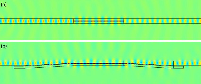
J. Phys. Photonics 3 (2021) 022009                                                                                           P Steglich et al

   Figure 8. Schematic of slot waveguide ring resonators: (a) fully slotted ring resonator; (b) partially slotted ring resonator
   and (c) cross-section of the slot waveguide phase shifter. Adopted from [86].

    An alternative strategy consists of exploiting the concept of a partially slotted ring resonator [94]. Here, a
slot waveguide is inserted into one of the straight sections of an elongated ring resonator (also called a
racetrack resonator), as shown in figure 8(b). This partially slotted ring resonator concept is a promising
candidate for integrating a SOH phase shifter into a ring resonator, keeping the optical loss at a very low
value. An extremely high device tunability of 700 pm V−1 was demonstrated using such a ring resonator
covered by a side-chain polymer system (poly[(methyl methacrylate)-co-(disperse red 1 acrylate)]) [32]. A
second advantage of this ring configuration is the reduced capacitance, which allows for an ultra-low energy
per-bit consumption of 87 aJ per bit [65]. Also, a 3 dB bandwidth at 1.34 GHz has been demonstrated, giving
rise to RF (radio frequency) modulators with low energy consumption.
    A second promising ring concept is based on subwavelength grating waveguides (SWG) [95–98]. Here,
the slot is introduced orthogonally to the direction of light propagation, instead of being parallel to it, as it is
usually realized. In 2018, Pan et al [99] demonstrated this concept to be appropriate for an EO modulator
with a 3 dB modulation bandwidth as high as 41.4 ± 1.1 GHz, while the device footprint was as small as
70 µm × 29 µm [95]. A device tunability of 41.28 pm V−1 was deduced from DC measurements. The
difference between the high tunability of a partially slotted ring resonator and the SWG is the fact that the
SWG-based ring resonator exhibits a significantly larger electrode gap. Figure 9 shows a schematic of an
SWG-based ring resonator, which has a racetrack configuration.

3. In-device performance of electro-optical polymers

3.1. Electro-optical effects in silicon-organic hybrid devices
In general, an EO polymer consists of a passive matrix containing active molecules with a strong EO effect.
The polymeric matrix gives the material its mechanical, thermal and chemical stability. In principle, active
molecules can be endowed with both linear and quadratic EO properties that can produce changes in
refractive index through the application of an electric field.
    Most EO devices based on organic linear EO materials rely on dipolar molecules embedded in, or
covalently bound to, the main chains of a usually amorphous polymer matrix. To act as a modulator under
the application of an external electric field E, a macroscopic non-centrosymmetric orientation of the dipolar
molecules has to be generated using an appropriate poling procedure [100]. The refractive index varies
linearly with the electric field E and the lack of inversion symmetry allows ∆n(−E) ̸= ∆n(E). This leads to a
linear EO (or Pockels) effect, which is appropriate for high-frequency application. However, the poling
procedure is sophisticated and prone to thermal instability and the reproducibility of the result is inadequate
for industrial applications. In spite of this, a huge amount of literature is available, on both the materials and
the devices [101–113].
    To overcome the intrinsic issues due to the linear EO effect, materials with a quadratic dependence of the
refractive index on the electric field can be exploited. In this case, no requirement of symmetry is necessary,

                                                         7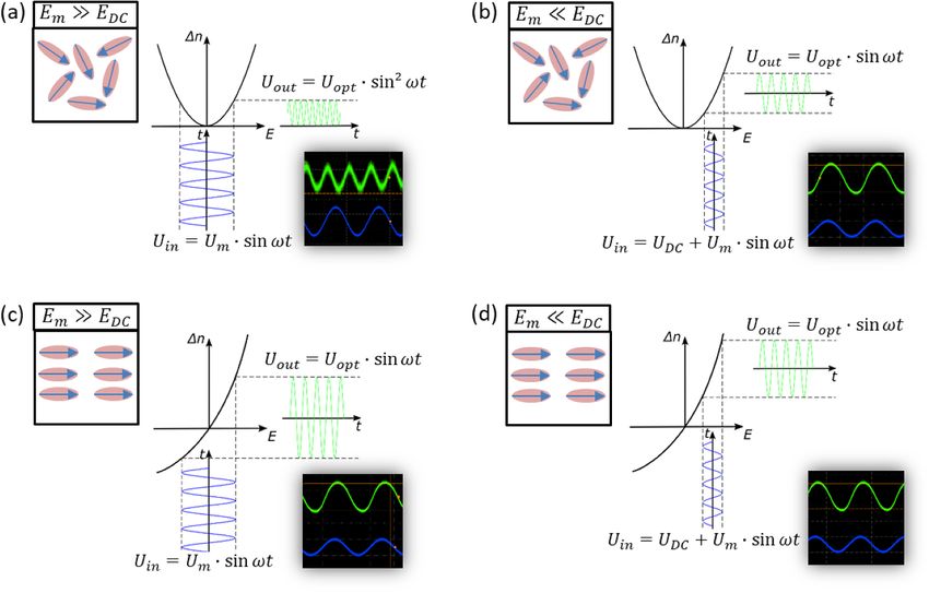
J. Phys. Photonics 3 (2021) 022009                                                                                     P Steglich et al

   Figure 9. Schematic of an SWG-based modulator. The photonic device consists of a ring resonator, which is coupled to an SGM
   bus waveguide. Yellow: the coupling region between the ring resonator and the bus waveguide. Blue: to reduce optical loss, a
   trapezoid SGM is used in bends at the four corners. In this way, a relatively high quality factor can be achieved. Red: a mode
   converter is employed to convert the optical mode of a conventional strip waveguide into the SGM mode and vice versa. © 2019
   IEEE. Reprinted, with permission, from [95].

because ∆n depends on E2 . All materials have a quadratic EO response; however, it is much smaller than the
linear response for non-centrosymmetric systems.
    The linear and quadratic EO effects have been intensively studied in bulk materials during recent
decades. Typically, each effect is considered separately, because the linear EO effect dominates in
non-centrosymmetric materials and vanishes in centrosymmetric materials. However, attention is required
when EO polymers are used in slot waveguides with narrow gaps (below 200 nm), as is typical for SOH
photonics. It has been shown that the quadratic EO effect has a noticeable contribution to the overall EO
effect, even in non-centrosymmetric materials [36]. Therefore, it is necessary to take both effects into
account.
    The microscopic polarization induced by an electric field can be described in terms of a Taylor series.
This leads to the field-dependent molecular dipole moment [114]:

                                        pi = µi + αij Ej + βijk Ej Ek + γijkl Ej Ek El + . . . ,                                    (1)

where µi is the static electric dipole moment, αij is the first-order polarizability, β ijk is the second-order
polarizability, and γ ijkl is the third-order polarizability. Note that this total dipole moment pi , taken per
average molecular volume, represents the molecular polarisation. Ej , Ek and El are the electric field
components. The higher-order polarizabilities in this series have also been called first- and
second-hyperpolarizability, respectively.
    The EO effect is usually described using the change of the optical indicatrix [115]:
                                               ( )
                                                  1
                                            ∆ 2        = rijk Ek + Rijkl Ek El ,                                                    (2)
                                                 n ij

where r ijk and Rijkl are the Pockels and Kerr coefficients, respectively, which describe the linear and quadratic
EO effects. In anisotropic materials and presuming a small change of the refractive index, the refractive-index
change ∆ni in the main direction of the optical indicatrix can be approximated by [114]:
                                                      1
                                               ∆ni ∼
                                                   = − n3i (rijk Ek + Rijkl Ek El ).                                                (3)
                                                      2
The EO effect can also be expressed using the non-linear susceptibility tensors as [36, 114]:
                                                          1 (2 )   3 (3 )
                                               ∆ni =        (χ Ek + χijkl Ek El ).                                                  (4)
                                                          ni ijk   2
                                                      8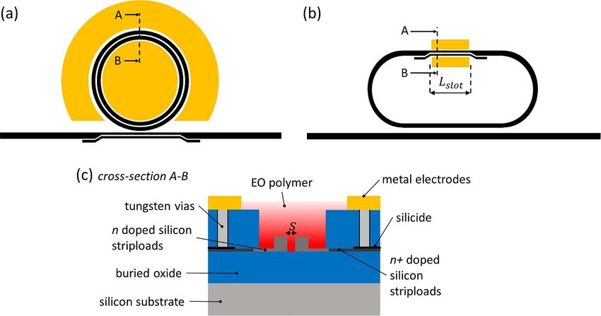
J. Phys. Photonics 3 (2021) 022009                                                                                  P Steglich et al

   Figure 10. D–π–A system. EO polymers are typically composed of electron-donating (D) and electron-accepting (A) side groups.
   Adopted from [38].

For SOH photonics, the special case of i = j = k = l = 3 is of particular interest in slot-waveguide structures.
                                                                    (2 )        (3 )
This is because it represents the dominant tensor components χ333 and χ3333 , where both input fields, i.e. the
optical and electrical fields, are polarized along axis 3. Therefore, this notation will be used throughout this
work. Further, we assume an isotropic refractive index, which is referred to as n. The EO tensors r ijk and Rijkl
                                                                           (2 )      (3)
are related to the second- and third-order susceptibility coefficients χijk and χijkl , respectively. Comparing
equations (3) and (4) yields the classical relations [36]:
                                                                       (2 )
                                                                   2χijk
                                                        rijk = −              ,                                                (5)
                                                                    n2i n2j

                                                                        (3 )
                                                                    3χijkl
                                                        Rijkl = −              .                                               (6)
                                                                    n2i n2j

3.2. In-device performance of the linear electro-optical effect
The linear EO tensor r ijk describes the EO activity of a non-centrosymmetric material and can be represented
in the case of guest–host systems by [114]:

                                                      rijk ∝ Nβ⟨cos3 Θ⟩.                                                       (7)

In equation (7), the chromophore number density or the number of non-linear molecules in the material
contributing to the polarization are denoted as N, and β represents the molecular first hyperpolarizability.
The average non-centrosymmetric order parameter is given by ⟨cos3 Θ⟩, where Θ denotes the angle between
the molecular dipole’s axis and the electric field vector. Equation (7) suggests that three approaches to
increase the linear EO effect are possible: (a) first, increasing the chromophore number density N; (b)
second, using chromophores with high first hyperpolarizability β; (c) third, maximizing the average
non-centrosymmetric order parameter ⟨cos3 Θ⟩ by inducing a high molecular orientation. EO polymers that
are dipolar and exhibit a highly polarizable donor–π–acceptor (D–π–A) system can meet such requirements.
In general, the D–π–A system can support charge transfer between electron-donating and electron-accepting
groups [116]. The electron donor groups mainly used in organic synthesis, are usually N(CH3 )2 , OCH3 , OH,
while the electron acceptor groups are mostly NO, O2 N, CHO, CN. The π–electron conjugated segment
serves to transmit the charge, as illustrated in figure 10. A poling procedure is required to obtain a
non-centrosymmetric molecular orientation and, hence, a large linear EO coefficient r 33 . In principle, the
procedure is as follows. First, the sample is heated from the ambient temperature (figure 11(a)) to nearly the
glass transition temperature of the polymer (figure 11(b)). Then, a relatively high voltage is applied to the
slot waveguide for several minutes (figure 11(c)). The electric field usually reaches a value in the order of
200 V µm−1 . This phase is followed by rapid cooling to ambient temperature while the poling voltage
continues to be applied (figure 11(d)). Finally, the active chromophores are aligned and fixed in their
orientation so that the poling voltage can be switched off (figure 11(e)). In principle, a further increase of the
EO effect in polymer systems with a non-centrosymmetric molecular orientation can be achieved by
operating them near to their absorption resonances, to make use of the so-called resonance enhancement of
the second-order effect [117]. A selection of widely used EO chromophores and polymers with a large linear
EO effect is shown in figure 12.
    Pan et al demonstrated a high-speed modulator based on the EO polymer SEO125. An EO coefficient r 33
of 54.7 pm V−1 was deduced from DC experiments. This, however, corresponds to a poling efficiency of only
43.8%, compared to the EO coefficient of the bulk EO polymer [95]. Further optimization of the poling
process is expected to improve this value.

                                                    9
J. Phys. Photonics 3 (2021) 022009 P Steglich et al
Figure 11. Poling procedure: at the beginning, the molecules are randomly orientated at the ambient temperature T a (a). The
sample is heated to the glass transition temperature T g of the polymer (b) and a voltage is applied to induce an electric field (c).
The chromophores are then aligned along the electric field, forming a non-centrosymmetric molecular orientation (d). The
sample is cooled to the ambient temperature, during which, the voltage is maintained. The molecular orientation is also retained
without a poling voltage (e), but molecular reorientation (relaxation) leads to long-term stability issues (f). Adopted from [36].
Figure 12. Structural formulas of widely used EO chromophores and polymers: (a) DLD164 [118], (b) MMA + PVT [119],
(c) PMMA + DR1 (guest–host system) [32], (d) PMMA + DR1 (side-chain system) [65], (e) JRD1 [120], (f) PSLD41 [85] and
(g) YLD124 [55].
10J. Phys. Photonics 3 (2021) 022009 P Steglich et al
One serious problem of the linear EO effect is its thermal and long-term stability due to orientational
relaxation dynamics (figure 11(f)) [101, 121]. However, recent advances in molecular engineering have led to
increased stability. For example, a cross-linkable EO system consisting of two chromophores (HLD1 and
HLD2 ) has been demonstrated to maintain 99% of the initial r 33 after being heated to 85 ◦ C for 500 h,
making it a promising candidate for future SOH modulators [122]. Kieninger et al studied a random
copolymer of four differently substituted methyl-methacrylate (MMA) moieties infiltrated into a silicon slot
waveguide [119]. This polymer system was introduced in 2016 [123] and exhibits a donor-acceptor-
substituted phenyl vinylene thiophene (PVT) chromophore as a side group, which is responsible for the EO
effect, while a bulky adamantyl side group increases the glass transition temperature. Using this polymer
system, high-temperature storage experiments at 85 ◦ C have been performed and an SOH modulator that
retained more than 85% of its modulation efficiency for at least 2400 h was presented. The device had a
voltage-length product of 3.3 V mm after the end of the experiment. This demonstrates the principle of the
reliability of SOH modulators at elevated temperatures, which complies with Telcordia standard
GR-468-CORE. However, this can only be achieved by using EO polymers with a high glass transition
temperature of 172 ◦ C [119]. In principle, the glass transition temperature needs to be significantly higher
than the operating temperature to avoid relaxation processes. Unfortunately, the most active EO polymers
exhibit glass transition temperatures between 80 ◦ C and 100 ◦ C. Therefore, a trade-off between EO activity
and long-term stability is necessary. However, a temperature budget of at least 400 ◦ C is required for the
integration of organic materials into a CMOS-compatible fabrication platform due to the use of
high-temperature annealing processes. To tackle this problem, novel organic EO materials have recently been
synthesized that show high thermal stability at temperatures of up to 315 ◦ C and their long term
electro-optic stability has been demonstrated for 300 h at 85 ◦ C [124].
The linear EO effect in polymers was widely used during the last decade in the development of SOH
modulators, as can be seen from table 1. From this table, it is apparent that Mach–Zehnder modulators were
mainly used to demonstrate high-speed modulation at line rates of up to 100 Gbit s−1 for OOK [77] and up
to 120 Gbit s−1 for PAM4 signals [79]. Also, SOH modulators based on slotted photonic crystal waveguides
have been demonstrated for use with EO modulation at a 40 GHz 3 dB bandwidth [54].
However, attention has to be paid to the reported r 33 values. The reporting of reliable EO data is only
possible if data analysis follows widely recognized methodologies or can be traced to accredited quantitative
structure–property relationships studied by independent laboratories. There are only a few publications that
provide deeper insights into the optical and EO properties of organic materials in slot waveguides. The first
investigation into thin films can further help to obtain a deeper understanding [125]. However, please note
that the values reported in the literature and, therefore, also in the present review, are in-device values,
meaning that the EO values are deduced from the device performance, but many physical effects such as
carrier accumulation or elasto-optical effects are neglected.
3.3. In-device performance of the quadratic electro-optical effect
More recently, a second category of devices has emerged, relying on the quadratic EO effect in SOH slot
waveguides. The quadratic EO effect is present in any molecular system irrespective of its orientation or
symmetry, which is an advantage in comparison with the linear counterpart. Moreover, the combination of
the quadratic EO effect with the optical Kerr nonlinearity in a slot waveguide is expected to pave the way for
various applications, e.g. electrically controlled multistable switches [137]. The main issue of the quadratic
EO effect is the relatively low response in terms of refractive index change as a function of the applied electric
field. However, the latest research has shown the feasibility of the quadratic EO effect for low-voltage
operation using an SOI slot waveguide phase shifter implemented in a micro-ring resonator [16, 86]. Due to
the fact that the quadratic EO effect depends quadratically on the electrode separation, s, it becomes highly
efficient in narrow slots, as plotted in figure 13.
There are several origins of the quadratic EO effect, e.g. electronic mechanisms, molecular
reorientational contributions, electrode attraction, and electrostrictive effects [138]. However, electronic
origins dominate the quadratic EO effect at room temperature because molecular reorientation is hindered
by the restraining force of the polymer, and electrode attraction is expected to be compensated for by the
elasticity of the polymer. Second-order electrostriction can be neglected in isotropic conjugated polymers, as
they are centrosymmetric and have no noteworthy dipole moment [139], and third-order electrostriction is
expected to have only a marginal influence. Consequently, the quadratic EO effect in conjugated polymers is
dominated by electronic mechanisms, which is of great interest in photonic applications due to its
exceptional bandwidth potential [140].
The main condition for a strong quadratic EO effect is that the electron system of the material should be
characterized by strong confinement. One example is polydiacetylene [141, 142], preferably in crystallized
11Table 1. Overview of current SOH modulators using the linear EO effect. MZ: Mach–Zehnder, RR: ring resonator, FS: frequency shifter, PM: phase shifter, OOK: on–off keying, SSB: single sideband modulation, QAM: quadrature
amplitude modulation, PAM: pulse-amplitude modulation, BPSK: binary phase-shift keying, QPSK: quadrature phase-shift keying, ASK: amplitude shift keying.
Device Polymer r 33 (pm V−1 ) Uπ L (V mm) Bandwidth (GHz) Signal W bit (fJ bit−1 ) Reference Year
MZ JRD1 — 0.41 — 100 GBd OOK and PAM4 — [126] 2020
J. Phys. Photonics 3 (2021) 022009
MZ SEO100 166 1.1 — 100 GBd 16QAM 25 [84] 2018
RR SEO125 54.7 — 41.4 — 2.5 [99] 2018
MZ PVT 80 3.3 20 40 Gbit s−1 OOK — [119] 2018
MZ SEO100 147 1.0 25 100 Gbit s−1 OOK 98 [77] 2018
MZ JRD1 390 0.32 43 40 Gbit s−1 OOK 8.5 [127] 2018
MZ SEO250 — 1.0 — 100 GBd 16QAM 30 [128] 2017
MZ SEO100 144 1.1 — 120 Gbit s−1 PAM4 100 [79] 2017
12
MZ JRD1 359 0.32 — 25 Gbit s−1 — [129, 130] 2017
MZ SEO100 110 1.1 — 50 Gbit s−1 OOK, 100 Gbit s−1 DB 160 [131] 2017
MZ SEO100 60 1.6 — 64 GBd 4ASK — [132] 2016
RR PMMA/ DR1 12.8 — — — — [32] 2016
FS DLD164 150 0.5 40 SSB — [118] 2016
PM YLD124/ PSLD41 230 0.45 >60 40 Gbit s−1 BPSK 70 [133] 2015
MZ SEO100 70 1.1 >60 40 Gbit s−1 OOK 225 [133] 2015
PM M3 18 11 >100 — — [134] 2014
MZ BNA 24 12 7 12.5 Gbit s−1 OOK — [78] 2014
MZ YLD124/ PSLD41 230 1.05 18 28 GBd QPSK, 16QAM 19 [55] 2014
MZ YLD124/ PMMA 30 4 18 40 Gbit s−1 OOK — [55] 2014
MZ PSLD41 98 1.22 18 40 Gbit s−1 OOK — [85] 2014
MZ YLD124/ PSLD41 230 0.52 18 40 Gbit s−1 OOK — [55] 2014
MZ DLD-164 — 10 11 10 GBd BPSK, 2ASK-2PSK — [135] 2014
MZ M3 15 2.7 10 10 Gbit s−1 OOK 320 [29] 2013
MZ M3 — 1.33 6.8 28 GBd 16QAM 640 [75] 2013
MZ M1 10 20 — 28 GBd BPSK, M-ASK 1000 [80] 2013
PM M1 230 11 90 56 Gbit s−1 QPSKJ. Phys. Photonics 3 (2021) 022009 P Steglich et al
Figure 13. Refractive index change induced by the quadratic EO effect as a function of the electrode distance, s, and the electric
field, E. The electric field is induced by applying a DC voltage U DC (E = U DC /s). The left highlighted region (green) refers to
typical values of slot waveguides, while on the right side (purple) typical values for bulk materials with electrode distances in the
micro-meter scale are plotted. It can be seen that the quadratic EO effect becomes effective at narrow electrode distances, as it is
possible with slot waveguides. © 2018 IEEE. Reprinted, with permission, from [65].
form, aligned with the axis of the one-dimensional conjugated electron system of the polymer chains in the
polarization direction of the traveling optical wave’s electric field vector. Other examples are conjugated azo
polymers such as poly[(methyl methacrylate)-co-(disperse red 1 methacrylate)] [65] or azo dyes such as
disperse red 1 (DR1), dicyanovinyl (DCV) and nitrofuran (NFAI) [143, 144]. In principle, short conjugated
oligomers and respective chromophores can also be used, e.g., beta carotene, oligoparaphenylenevinylene,
and oligocyaninedyes but also more stable ladder-type polymers such as oligorylenes or ladder-type
polyparaphenylene [145].
An alternative to these organic materials is represented by composite materials which are composed of a
transparent dielectric matrix filled with a suitable concentration of one-dimensional conductive or
semi-conducting nano-domains, which also exhibit the required confinement of the electron system. Some
examples are gold, silver, tungsten, aluminum or metallic or semiconducting nanowires, and also formed and
aligned nanodots which have direct contact with each other. The matrix materials can be dielectric polymers,
glass or various dielectric oxides e.g. silicon dioxide or other suitable oxides e.g. hafnium dioxide. In
addition, certain inorganic materials can be used, e.g. salts such as sulfides, bisphosphonates or nitrates. In
this case, the crystallographic axis with the highest linear polarizability and hyperpolarizability should be
aligned to a sufficient extent with the polarization direction of the electrical field used for modulation. Other
promising materials are ferroelectrics such as potassium lithium tantalate niobate K1 − y Liy Ta1 − x Nbx O3
(KLTN) [146] and materials based on CsPbBr3 nanocrystals [147].
Recently, the first RF modulator based on the quadratic EO effect in poly[(methyl methacrylate)-
co-(disperse Red 1 methacrylate)] was demonstrated with a 3 dB bandwidth of 1.34 dB [65]. This SOH ring
resonator modulator was realized using a photonic integrated circuit (PIC) technology on a 200 mm wafer,
demonstrating wafer-scale fabrication of SOH devices. An exceptionally large device tunability of 350
pm V−1 was achieved, surpassing state-of-the-art silicon modulators by an order of magnitude. Moreover,
the ring resonator has an advanced design to obtain an ultra-low per-bit energy consumption of 87 aJ bit−1 .
This demonstrates the potential of the quadratic EO effect to be used in high-performance photonic devices
with low energy consumption.
A method for determining the dispersion of the third-order susceptibility and the molecular
hyperpolarizability of a SOH slot waveguide ring resonator is presented in [86]. Here, a two-level model is
used to determine the dispersion of the third-order hyperpolarizability of a linear conjugated molecule in the
off-resonant spectral region (the optical C-band). Poly(methylmethacrylate) doped with 5 wt% DR1 was
employed to evaluate the quadratic EO coefficients R11 and R12 . Figure 14 shows the observed quadratic EO
coefficients. Note that the values of R11 were experimentally obtained (black dots) and fitted using a
least-squares fitting procedure (red line), while the values for R12 were evaluated from R11 using the relation
R11 = 3R12 . However, it is worth highlighting that the ring resonator used was fabricated with an SOI
technology, which allowed the evaluation of the on-chip performance of novel EO materials using the same
technological conditions as those used for the final device.
13J. Phys. Photonics 3 (2021) 022009 P Steglich et al
Figure 14. The plotted values of R11 in (a) and (b) are observed experimentally and then fitted. The values of R12 in (c) are
evaluated using the values of R11 of (a) by assuming a two-level model and that the electronic mechanisms dominate in the
off-resonant spectral region. Adopted from [86].
Figure 15. (a) Resonant wavelength shift as a function of the applied voltage before and after applying a poling procedure.
(b) Nonlinear optical susceptibilities deduced from the resonance shift. Adopted from [36].
So far, both EO effects have been considered separately, because the quadratic EO effect is
significantly weaker compared to the linear EO effect. Classically, the quadratic EO effect is neglected in
non-centrosymmetric materials. However, investigations have been undertaken to show that the quadratic
EO effect is not only sufficiently strong enough in SOI slot waveguides using a centrosymmetric molecular
order, but also contributes to the overall EO effect in non-centrosymmetric materials. In [36], it was revealed
that the quadratic EO effect contributes 32% to the overall EO effect. Figure 15(a) shows the experimentally
observed resonance wavelength shift of the ring resonator caused by applying an electric field to the SOI slot
waveguide. The experiments were performed before and after a poling procedure was applied to the EO
material. The non-linear optical susceptibilities are deduced from the curves in figure 15(a) and plotted in
figure 15(b). This finding suggests that the overall EO effect should be separated into linear and quadratic
contributions to avoid an overestimation of the linear EO coefficient in non-centrosymmetric materials.
14J. Phys. Photonics 3 (2021) 022009 P Steglich et al
Figure 16. Various EO responses in SOH photonic devices under different conditions: (a) If Em ≫ EDC and χ(2) ≈ 0, the electric
modulation field (blue) induces a sine squared modulated optical field (green). (b) χ(2) is equal to zero if the symmetry is broken.
The electric modulation field (blue) then causes a sine modulated optical field (green) as well as a refractive index offset. (c) If
Em ≪ EDC , i.e., an offset voltage is applied, and the modulation amplitude is small enough, the modulated optical response is
observed as a sine function. (d) An offset voltage also provides a larger refractive index offset in acentric materials but also a larger
EO response due to the slightly non-linear response curve. Adopted from [36].
Furthermore, the influence of both EO effects on intensity modulation was investigated in [36]. As shown in
figure 16, the simultaneous use of both EO effects can lead to different modulation schemes. This gives rise to
novel concepts for reconfigurable and field-programmable photonic devices.
3.4. In-device performance of the electric-field-induced linear electro-optical effect
Silicon also exhibits a relatively large third-order optical susceptibility χ(3) [148]. Unfortunately, this is
accompanied by nonparametric processes such as two-photon absorption (TPA) and free-carrier absorption
(FCA) at the optical intensities required in the telecommunications wavelength bands. The heterogeneous
integration of materials with high χ(3) and insignificant TPA and FCA has been pursued to avoid that
shortcoming. For example, chalcogenide (ChG) glass [149], Hydex [150], Si3 N4 [151], and hydrogenated
amorphous silicon (a-Si:H) [152] are some of the major non-organic materials that have been employed
recently.
However, the major advantage of organic materials, compared to silicon, is their negligible
nonparametric processes (TPA, FCA). Therefore, third-order non-linear effects are also of great interest in
the development of SOH photonic devices. One promising third-order effect in organic materials is the
electric-field-induced linear EO effect, which is based on χ(3) and has been recently revealed in polymers and
an SOH ring resonator [153].
It is induced by applying a static electric field in addition to a time-varying (modulated) electric field:
E = EDC + Em sin(ωt), (8)
where EDC is the static electric field and Em sin(ωt) denotes the modulation field. All fields are evaluated by
the applied voltage and slot width (E = U/s). Inserting equation (8) into the refractive index change
(quadratic EO effect):
1 3 (3)
∆n = χ (−ω; ω, 0, 0)E2 , (9)
n 2 3333
leads to
3 χ (3) 2
∆n = [EDC + E2m sin2 (ωt) + 2EDC Em sin(ωt)]. (10)
2 n
15J. Phys. Photonics 3 (2021) 022009 P Steglich et al
Figure 17. (a) Dependence of the modulated optical amplitude I m on the modulation amplitude Em and at different static electric
fields EDC . (b) Dependence of the modulated optical amplitude I m on the static electric field EDC and with the modulation
amplitude Em as a parameter. © 2020 IEEE. Reprinted, with permission, from [153].
The first term does not influence the EO modulation, since it is a constant. However, it is expedient to
distinguish between the two cases. On the one hand, if Em ≫ EDC , the third term in equation (10) can be
neglected. Consequently, the optical signal follows a sine-squared relation (E2m sin2 (ωt)). On the other hand,
the second term can be neglected and the observed signal is dominated by the third term if Em ≪ EDC , which
follows a simple sine relation (2EDC Em sin(ωt)). This case is referred to as the electric-field-induced linear EO
effect. Here, the third-order susceptibility χ(3) is efficiently translated into an electric-field-induced
(2 )
second-order susceptibility χEFI = 3χ (3) EDC [154].
To validate the electric-field-induced linear EO effect in SOH devices, it is reasonable to distinguish the
modulated optical signal in two cases. Here, the measured output intensity (I out ) of an optical resonator can
be observed as:
3χ (3) 2
Iout = Im sin2 (ωt) ∝ E sin2 (ωt), (11)
2n m
if EDC ≪ Em or
(2 )
χEFI
Iout = Im sin(ωt) ∝ Em sin(ωt), (12)
n
if EDC ≫ Em , where I m refers to the detected intensity in terms of the modulation amplitude.
First, a sinusoidal input signal Em sin(ωt) is applied without a static electric field, i.e. without an offset
voltage, to validate equation (11). In this case, the modulation amplitude is set to a fixed value. In a further
experiment, equation (12) is confirmed by applying a static electric field induced by an offset voltage in
addition to a modulation amplitude.
One unique feature of the electric-field-induced linear EO effect is the linear dependency of the
modulation amplitude Em on the modulation optical amplitude I m . Figure 17(a) shows the intensity
amplitude, Im , obtained as a function of the observed amplitude Em , using different static electric field
strengths, EDC . Large modulation fields Em (>2.8 V µm−1 ) lead to a non-linear response. As a consequence,
only the parameter space in which the modulation is purely linear is fitted in figure 17(a). However, a change
of the static electric field strength EDC leads to an increase in the slope of the graph in figure 17(a).
Figure 17(b) shows the modulated optical amplitude I m as a function of the static electric field EDC and the
modulated electric field amplitude Em as a parameter. From this figure, it is apparent that the static electric
field EDC has an impact on the modulated optical amplitude I m . The linear dependence of the optical output
amplitude on the static electric field gives rise to novel applications. In particular, this approach is a
promising candidate for an EO modulator with adjustable amplitude, or as an optical attenuator that does
not require additional photonic components. It is also notable that extremely efficient electric-field-induced
second-harmonic generation (EFISH) has recently been demonstrated in an EO polymer [155]. This could
be another approach for future SOH photonic devices.
16J. Phys. Photonics 3 (2021) 022009 P Steglich et al
Figure 18. Cross-sectional view (focused ion-beam image) of a strip-loaded slot waveguide in a PIC technology. Adopted from
[71].
Figure 19. (a) Slot waveguide covered by silicon dioxide and silicon nitride layers with thicknesses of 10 nm and 100 nm,
respectively. (b) Back end of line (BEOL) to connect the doped silicon strip loads with the first metal layer and with planarizing
silicon dioxide layers after deposition and chemical-mechanical polishing (CMP). (c) First metal layer structured by reactive ion
etching (RIE) over a resist mask. (d) RIE up to the silicon nitride sheet (thickness of 50 ± 20 nm) to structure the cavity.
(e) Structuring the last part of the cavity by removing the silicon dioxide within the slot using wet etching. (f) Slot waveguide
filled with organic material by spin coating. Adopted from [156].
4. Overview of CMOS integration concepts and future aspects
The main challenge for future SOH devices is their integration into CMOS-compatible process flows. The
iIndustrial adoption of SOH devices can be achieved using PIC technology. For example, this can be realized
as a modular part of a complex SiGe-BiCMOS platform [65, 156]. This technology uses either an SOI wafer
or a local SOI on a bulk silicon wafer for the monolithic integration of photonic and electronic devices.
Figure 18 shows a focused ion image of a slot waveguide in such a technology. The slot waveguide is
connected through doped silicon strip loads and tungsten vias to aluminum electrodes. The slot waveguide
needs to be released from the SiO2 -cladding to deposit an EO polymer inside the slot by spin-coating.
Therefore, the process flow is interrupted for simplicity after structuring the first metal layer instead of
fabricating the complete back-end of line (BEOL) with five metal layers. To release the silicon slot waveguide,
the SiO2 -cladding is locally removed using an etching procedure [156, 157]. The complete release process is
schematically shown in figure 19. First, the front-end of the line (FEOL) is finished (figure 19(a)). At this
point, the slot waveguide is covered by silicon dioxide and silicon nitride layers with thicknesses of 10 and
100 nm, respectively. The BEOL is fabricated until the first metal layer is the next step, as shown in
17J. Phys. Photonics 3 (2021) 022009 P Steglich et al
Figure 20. (a) Top and (b) cross-sectional views (focused ion-beam image) of a strip-loaded slot waveguide in PIC technology.
Adopted from [71].
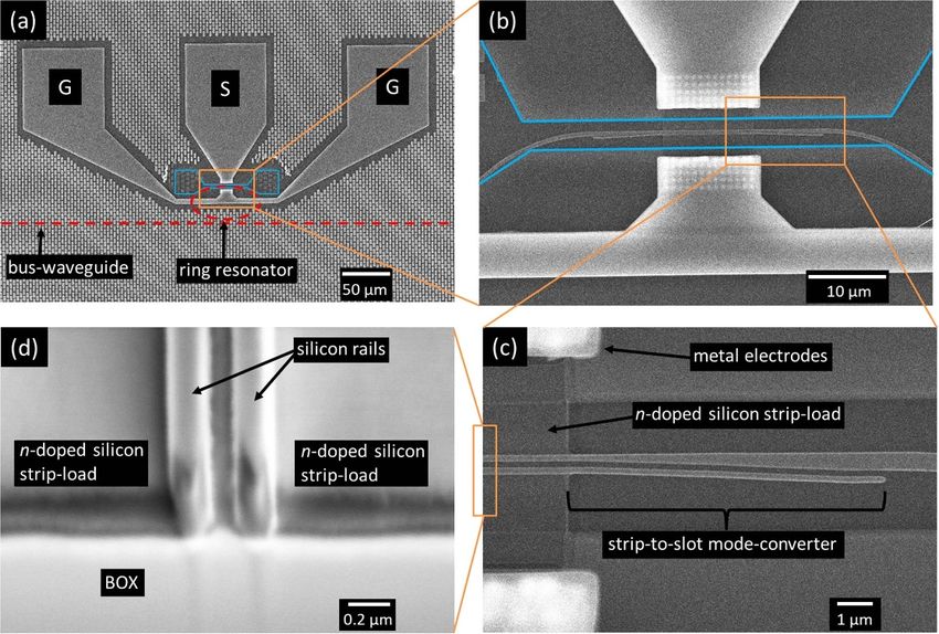
Figure 21. (a) Secondary electron microscopic (SEM) image of the ground–signal–ground electrodes from the above with a
trench (highlighted in blue) to deposit the EO polymer inside the silicon slot waveguide. The ring resonator and bus waveguide
are shown by a dashed red line. (b) Magnification of the ring resonator with strip-to-slot mode converter and slot waveguide.
(c) Magnification of the strip-to-slot mode converter. (d) Details of the strip-loaded silicon slot waveguide. © 2018 IEEE.
Reprinted, with permission, from [65].
figures 19(a) and (b). Chemical–mechanical polishing (CMP) steps are employed to get a planar topography
of the deposited silicon dioxide layers. The metal electrodes are deposited on top of the silicon dioxide layers
and structured by reactive ion etching (RIE) using a hard mask. A further resist mask is used to remove the
silicon dioxide stack above the slot waveguide by RIE (figure 19(d)). It turns out that this process step is
challenging, because the oxide stack above the wafer has relatively low uniformity in terms of etching speed.
Therefore, an RIE process that is very selective to silicon nitride is used to overcome this issue. The silicon
dioxide is removed up to the silicon nitride layer. The remaining silicon nitride is etched using RIE with high
selectivity to the underlying oxide. Finally, the silicon oxide is removed with a wet-etch process to completely
release the slot waveguide (figure 19(e)). The EO polymer is then deposited by spin-coating (figure 19(f)).
Further details of the fabrication process can be found in [71, 156, 157]. Figure 20 shows a slot waveguide
fabricated in a 0.25 µm SiGe BiCMOS pilot line following the fabrication scheme in figure 19 [65]. It is
apparent from this figure that the slot waveguide is completely released. However, the tungsten vias and
metal electrodes are partly disconnected because of the relatively long wet-etch procedure, which induces
stress due to the missing oxide below the metal electrodes. This, in turn, reduces the device’s performance,
since the resistance is drastically increased . Further developments are necessary to tackle this problem, which
is the subject of ongoing research. However, this technology was first translated into a working device in 2015
18You can also read