Development of microelectrodes for electrical measurements in a microfluidic system
←
→
Page content transcription
If your browser does not render page correctly, please read the page content below
Development of microelectrodes
for electrical measurements in a
 microfluidic system

 Emma Thomée
 2017

 Master’s Thesis in Biomedical Engineering
 Faculty of Engineering LTH

 Department of Biomedical Engineering

 Supervisor: Lars Wallman
 Assistant supervisor: Anette Wolff
Abstract

Transendothelial electrical resistance (TEER) measurements are used to
quantitatively monitor cell barrier formation in in vitro models of the blood-brain
barrier. TEER measurements in microfluidic in vitro systems are technically
problematic and have suffered from poor measurement reproducibility.
The aim of this Master’s thesis project was to develop fully integrated electrodes
for measuring TEER in a microfluidic blood-brain barrier model. Two patterns of
thin film electrodes – one with electrodes placed in the microfluidic channels, and
one with electrodes directly above and below the cell culture membrane – were
designed, fabricated and embedded in the microfluidic system. Electrodes were
fabricated in silver and in platinum, and their reproducibility was evaluated using
impedance spectroscopy.
Results showed that electrodes fabricated in platinum and placed directly over the
membrane could measure impedance with the highest precision. Measurement
variation from the electrodes placed in the channels was shown to effectively be
reduced by employing a technique of combining six measurements from four
electrodes. Based on the reproducibility studies presented in this report, both types
of electrodes were believed to have sufficient sensitivity and robustness to be used
for TEER measurements.
A robust technique to measure TEER enables real-time monitoring of cells in
microfluidic systems, and offers a quantitative validation parameter for easy
comparison and benchmarking of different system.

Acknowledgements
First of all, I wish to thank my supervisor Lars Wallman and assistant supervisor
Anette Wolff at the department of biomedical engineering at Lund University.
They have both provided invaluable guidance, support and enthusiasm throughout
this project. I also wish to thank Martin Bengtsson for teaching me the fabrication
processes and assisting during all work carried out in the cleanroom facilities.

At Uppsala University I would like to thank Maria Tenje and the members of the
research team EMBLA for welcoming me as a member of the team and for giving
me valuable feedback and encouragement. During the project I also got the
opportunity to travel to Uppsala to meet with the team and take part of two days
of scientific exchange.

Last but not least, many thanks to the staff at Biomedical Engineering for helping
and sharing their expertise, as well as for instructing and assisting me in the
laboratories.
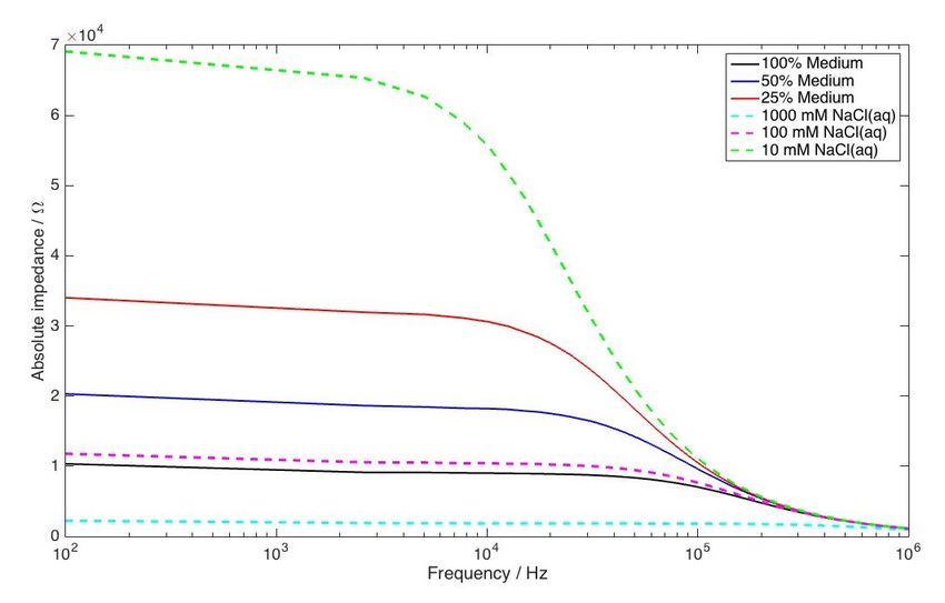
Table of contents
1. Introduction .................................................................................................. 1
2. Project background and research questions ...................................... 3
3. Theoretical Background ............................................................................ 5
 3.1 The blood-brain barrier ....................................................................... 5
 3.2 BBB In vitro ............................................................................................ 7
 3.2.1 Validation of in vitro models ........................................................... 7
 3.2.2 The next generation of in vitro models: organs-on-chips .......... 7
 3.3 Transendothelial electrical resistance ............................................ 8
 3.3.1 TEER measurements in vivo ......................................................... 9
 3.3.2 TEER measurements in vitro ......................................................... 9
 3.4 Impedance Spectroscopy ................................................................. 11
 3.4.1 Electrical impedance spectroscopy for TEER measurements 12
 3.5 Microfabrication .................................................................................. 13
 3.5.1 Electrode properties ...................................................................... 14
 3.5.2 Electrode fabrication techniques ................................................. 14
4. Method ......................................................................................................... 16
 4.1 Literature study ................................................................................... 16
 4.2 Electrode design ................................................................................. 16
 4.3 Fabrication ............................................................................................ 18
 4.3.1 Fabrication of electrodes with photolithography ....................... 18
 4.3.2 Assembling the device .................................................................. 20
 4.4 Electrical Impedance Measurements............................................. 21
 4.4.1 Measurement procedure .............................................................. 21
5. Results ......................................................................................................... 23
 5.1 Literature study ................................................................................... 23
 5.2 Electrodes ............................................................................................. 25
 5.3 Impedance measurements: square electrodes........................... 26
5.3.1 Characterisation of electrodes in single-channel prototype
 device ........................................................................................................ 27
 5.3.2 Silver electrodes vs. platinum electrodes................................... 29
 5.3.3 Characterisation of assembled chips .......................................... 32
 5.3.4 Sensitivity test ................................................................................ 33
 5.3.5 Reproducibility test ........................................................................ 33
 5.4 Impedance measurements: ring electrodes ................................ 35
 5.4.1 Characterisation of an assembled chips .................................... 35
 5.4.2 Sensitivity test ................................................................................ 37
 5.4.3 Reproducibility test ........................................................................ 37
6. Discussion .................................................................................................. 40
 6.1 Possibilities to derive TEER ............................................................ 42
 6.2 Ethical reflection ................................................................................. 44
7. Conclusions and future aspects ........................................................... 45
8. Appendices ................................................................................................. 47
 Appendix A – Microfabrication protocols ........................................... 47
 A1. Mask fabrication ................................................................................ 47
 A2. Spin coat negative resist on glass wafer....................................... 47
 A3. UV lithography................................................................................... 47
 A4. Development of photoresist ............................................................ 48
 A5. Metal deposition and Lift-off ............................................................ 48
 Appendix B – Impedance Measurement Protocol ............................ 49
10. References ................................................................................................ 51
1. Introduction
By combining the principles of microfluidics, microfabrication and cell culturing
techniques, a new type of laboratory platforms has emerged, known as “organs-
on-chips”. Organs-on-chip systems are microengineered devices containing living
cells. Their purpose is to model structure and behaviour of human organs [1].
Among other applications, these systems can be used as screening platforms in
the pharmaceutical industry, providing an alternative to animal testing [2]. They
have the potential advantage of being easy and cheap to manufacture in large scale
while avoiding the ethical issues associated with the use of laboratory animals.

One type of biological structure that has been modelled on a microfluidic chip is
the blood-brain barrier (BBB). Previous studies have shown that microfluidic
models of the BBB can provide more realistic microenvironments compared to
earlier in vitro models [3]. A BBB-on-chip is typically made up of two-layered
crossing microchannels with endothelial cells cultured on a permeable membrane.
These systems show great potential in proof-of-concept studies, but a remaining
challenge in the field is the lack of standardisation when measuring quantification
parameters [4]. This makes it difficult to compare and benchmark models to other
existing models.

The most used parameter to quantitatively evaluate barrier quality in BBB-models
is transendothelial electrical resistance, commonly shortened TEER. TEER is a
measurement of how much the cellular barrier impedes an applied electrical
current, which relates to the quality of the barrier. The concept of TEER is simple
and well defined. However, there is inconsistency in the measurement procedure
and setup. This has been identified as a contributing factor to the large
measurement variability of TEER that has been reported in literature [5].

This Master thesis project aims to develop a robust measurement technique to
measure TEER in a BBB-on-chip system. Electrodes were developed and
integrated in the device, and evaluated by impedance spectroscopy measurements.
The report describes and discusses the processes and results of designing,
fabricating and characterising the electrodes.

 1
2
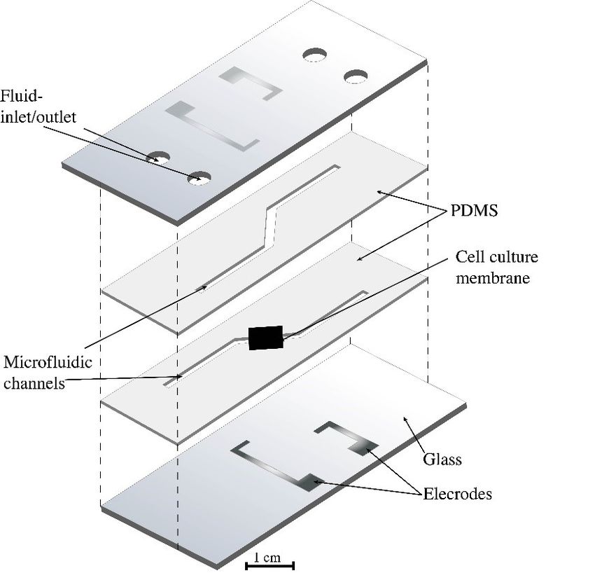
2. Project background and
research questions
This master thesis project is a collaboration with an on-going research project
aiming to develop a BBB-on-chip model. The principal goal of this thesis is to
develop integrated electrodes for measuring TEER. Electrodes are primarily
developed to be integrated in this device, but with the ambition to also be
implementable in other two-layered channel systems separated by a membrane.
This project sets out to be a first experimental study about electrical measurements
on the device, laying the groundwork for future studies. The resulting components
aim to be used in research.

The following research questions constitute the framework of the project:

 1. Can integrated electrodes provide stable and reproducible impedance
 measurements?
 2. How can the electrode design and measurement set-up be optimised to
 reduce measurement related variations?
 3. Can the integrated electrodes be used to measure TEER in a microfluidic
 BBB-model?

The device, which has been developed at the department of biomedical
engineering at Lund University, is made up of two layers of polydimethylsiloxane
(PDMS), each comprising a 500 μm high channel. Where the two channels
overlap, a thin, permeable membrane for endothelial cell seeding is embedded,
allowing diffusion between the channels through the membrane and the
monolayer of cells. Free diffusion is assumed across the membrane. The PDMS
layers are positioned between two layers of glass. Each channel has a fluid
inlet/outlet connected form the top of the chip. The device is expected to hold flow
rates around 920 mL/h, corresponding to the flow needed to reach physiological
sheer stresses [6]. An illustration of the chip at the start of the project is presented
in figure 2.1.

 3
1 cm
Figure 2.1: Illustration of the BBB-on-chip model at the start of the project.

 4
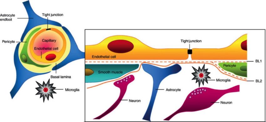
3. Theoretical Background

This chapter summarises the theoretical background information that the project
is based on. The biology of the human BBB is shortly presented, followed by a
description of BBB in vitro models and TEER measurements. The final sections
discuss electrical impedance spectroscopy and microfabrication techniques that
were used in the project.

3.1 The blood-brain barrier
The BBB is the boundary layer of specialised endothelial cells that separates blood
from brain interstitial fluids. They make up the blood vessels in the brain. The
endothelial cells of the BBB are surrounded by a basement membrane and four
other types of cells: astrocytes, pericytes, neurons and microglia. These five types
of cells and the basement membrane together make up the neurovascular unit
(figure 3.1) [7].

Figure 3.1: A schematic image of the neurovascular unit, showing its five types of
cells [7].

The main function of the BBB is to act as a physical and metabolic barrier by
allowing selective transport of nutrients through, but preventing toxic substances
in the blood from entering the brain. There are two main pathways for transport
across the BBB (figure 3.2) [8]:

 5
1) the transcellular pathway
2) the paracellular pathway.

Figure 3.2: A schematic image of the BBB, showing the paths of transport across
the barrier.

The specialised endothelial cells differ from normal endothelial cells as they are
positioned very close to each other. Sealing protein complexes called tight
junctions are formed between adjacent cells. As a result, cells are held in close
proximity to each other, thereby occluding the intracellular spaces and preventing
transport through the paracellular pathway. Transport across the transcellular
pathways is regulated by transport proteins which is very selective, only allowing
specific substances to cross. Small molecules, such as oxygen and carbon dioxide,
can passively diffuse across the BBB [8].

This high barrier tightness is characteristic of the BBB, and crucial for maintaining
brain homeostasis. A local disruption of tight junctions, disrupting the barrier
tightness resulting in a leakage through the BBB, is associated with several
diseases of the central nervous system (CNS) [9]. Understanding and overcoming
the BBB is essential for treatment of diseases on the CNS. Drug delivery systems
that can temporarily open the barrier, allowing medication to pass through and
reach the brain, is a key research area for the treatment of CNS diseases.

 6
3.2 BBB In vitro
In vivo studies of the whole brain performed on laboratory animals have provided
useful information about the BBB. The main advantage of in vivo models in the
form of laboratory animals is that the brain can be studied in its natural, complex
environment [10]. However, due to ethical issues and poor conformance to the
human brain, research has put effort into mimicking the human brain environment
in vitro, based on cell culture techniques [11]. In artificial environments
conditions can be kept under high control and specific behaviours can be
independently studied with little interference of other factors. In vitro models can
be produced at low cost and can therefore be used for high throughput
experiments. Traditionally, the BBB has been reconstructed in vitro as two-
dimensional, static models. However, microfluidic organs-on-chip models are
now progressing as an applicable alternative [12].

3.2.1 Validation of in vitro models

Essential questions when developing BBB in vitro models are: “How do we know
that the model is a good representation of the physiological BBB?” and “How can
we ensure that the barrier is tight enough to study the permeability of different
substances?”. There are several methods to validate the barrier tightness of BBB
models. No one technique alone is good enough to characterise the barrier
tightness, but combining several qualitative and quantitative measurements can
give a good indication. Commonly used qualitative validation methods include
fluorescence microscopy and western blot. The most used quantitative parameters
for validation are permeability measurements of solutes and TEER measurements.
Although most microfluidic BBB models have been evaluated by measuring the
TEER, far from all models have [12]. Possibly, TEER measurements are excluded
from some studies due to uncertainties around how to properly measure it.

3.2.2 The next generation of in vitro models: organs-on-chips

Recently, BBB models based on organs-on-chip technology have become a
prominent class of in vitro models. BBB-on-chip models show several advantages
over the traditional two-dimensional, static models. The static BBB models, such
as the popular and commercially available Transwell cell culture insert (Corning
Inc., Corning, NY), consists of a membrane suspended in a well of cell culture
medium where endothelial cells are usually grown on top of the membrane (figure
3.3). Although these models are fit for many types of cell studies, they are often
too simple and fail to replicate parts the physiological environment [3]. Organs-

 7
on-chips however, can be designed with more realistic architectures. Their small
dimensions better represent the geometry of the capillaries in the neurovascular
unit. Bringing cell cultures down to the microscale minimises the number of cells
needed, resulting in lower operation costs. Further, by employing microfluidics
instead of conducting experiments in a bulk solution, the models can display
physiological phenomena such as fluid flows and shear stresses. Another
advantage of BBB-on-chip models is that sensors for real-time monitoring can be
integrated [2].

Figure 3.3 Illustration of a Transwell cell culture insert. A monolayer of
endothelial cells are cultured on top of a membrane.

3.3 Transendothelial electrical resistance
TEER describes the resistance across a cellular barrier, and is often used as a
validation tool to control if endothelial cells in BBB models form tight junction
complexes [4]. If the endothelial cells are growing properly and form tight
junctions to adjacent cells, the intercellular spaces of the cell layer are occluded
and the flow of current through is restricted [13]. This induces a higher resistance
to current, which is reflected in higher TEER values. TEER is often expressed
normalised to the membrane area in the unit Ωcm2, as in formula 1 below, to
facilitate direct comparison to other models.

 (Ω 2 ) = (Ω) × ( 2 ) (1)

The concept of TEER was first introduced by Crone et al. in 1982 [14], when they
measured the voltage drop along frog vessels. In BBB models, measuring TEER

 8
is a quick, non-invasive method enabling real-time evaluation of the quality of the
barrier. The measurements are performed by applying a low electrical current
across the cellular layer, while measuring how much the current is impeded by the
cell layer.

3.3.1 TEER measurements in vivo

TEER measurements have been performed in vivo in frogs and rats, with a derived
average TEER of 1840 Ωcm2 [14] and 1500 Ωcm2 [15] respectively. The same
measurements performed in mesenteric capillaries, on cells that do not from tight
junctions, gave TEER results in the range of 1-3 Ω cm2 [14]. This significant
difference in TEER between cells that form tight junctions and cells that do not
from tight junctions, demonstrates the effectiveness of TEER as a method of
monitoring tight junction formation. Due to ethical reasons, these measurements
have not been performed on the human body, and the specific TEER values of the
human BBB are thus unknown.

3.3.2 TEER measurements in vitro

TEER measurements are performed on both static and microfluidic BBB in vitro
models. In static models, TEER can be measured by inserting chopstick electrodes
to both sides of the membrane and measure resistance before and after the cells
form tight junctions. The resistance measured before makes up the baseline of the
system, and is subtracted from the resistance measured after, in order to isolate
the TEER value that is caused by the formation of tight junctions. Although there
are well-established measurement protocols for this type of measurement in static
models, there are limitations to both the measurement setup and the biological
relevance of the results. Static models fail to recapitulate the biological feature of
fluid flow. As there is no fluid flow present, the cells are not exposed to shear
stresses, which is expected to influence the cell differentiation and enhance the
formation of tight junctions [16]. Regarding the measurement setup, chopstick
electrodes are criticised for uneven distribution of current flow, especially in large
chambers [17]. Further, the measurements are vulnerable to movement of the
chopstick electrodes which makes it difficult to repeat measurements, causing
large variances between measurements. Alternatively TEER can be measured
with commercially available systems specifically developed to measure TEER,
such as Endohm cups (WPI inc), Millicell® inserts (EMD Millipore) and the
CellZscope® (NanoAnalytics) system.

TEER measurements are also challenging to perform in microfluidic models. Due
to their small geometries, chopstick electrodes are too large to fit inside the
systems. The commercially available TEER measurement systems previously

 9
mentioned are primarily developed for the Transwell insert and not compatible
with microfluidic models. These systems can therefore not measure TEER of
microfluidic models in situ, and thereby only give indirect estimations of the
TEER in the device. Recently, efforts have been made to integrate electrodes in
the microfluidic device to measure TEER in situ [18] [19]. A summary of TEER
values in literature measured by integrated electrodes is presented in table 3.1.

 Article/Reference Cell type Methods TEER
 ( Ωcm2 )
 Henry et al. hAECs - Gold thin film 121 ± 6
 (2017) [19] electrodes (± SEM)
 - 4-point configuration,
 impedance
 spectroscopy
 van der Helm hCMEC/d3 - Platinum wire 22 ± 1.3
 et al. (2016) [20] electrodes in channels (± SEM)
 - 2-point configuration,
 multiple paths
 impedance
 spectroscopy
 Griep et al. (2013) hCMEC/d3 Platinum wire 36.9 ± 0.9
 [21] electrodes (± SEM)
 2-point configuration,
 impedance
 spectroscopy
 Booth et al. bEnd.3 - Ag/AgCl thin film 223
 (2014) [18] electrodes
 - 4- point configuration,
 resistance
 measurements
 Douville et al. bEnd.3 - Ag/AgCl electrodes ≈150-200
 (2010) [22] - 2-point configuration,
 impedance
 spectroscopy
 Wang et al. BMECs in - Ag/AgCl electrodes Monoculture:
 (2016) [17] monoculture- 4-point configuration, 368 ± 60
 and coculture resistance (± SD)
 measurements Coculture:
 > 2000
Table 3.1 Summary of TEER values measured from integrated electrodes reported
in literature

 10
Like in the static models, TEER measurements in microfluidic models have
suffered from measurement variabilities and low sensitivity. It has been pointed
out that TEER measured in microfluidic models differ from TEER measured in
Transwell models using the same cell line [5]. It remains a challenge to produce
stable TEER results that can be reproduced in a robust manner. A prominent
source of measurement variability appears in microfluidic models with long and
narrow channels. This is because the resistance of the medium in the channels is
often in the same order of magnitude as, or higher than, the resistance across the
cell layer. Medium inhomogeneity, due to change in temperature or concentration,
affects the resistivity and can thus significantly affect the TEER readout [20].
Additionally, as a consequence of the high channel resistance, small movements
of electrodes may cause a relatively large change in total measured resistance of
the system. However, many sources of variation can be eliminated with a robust
measurement setup [5].

In vitro models of the BBB need to reach TEER values above 150-200 Ωcm2 to
be considered acceptable models [23]. This is approximately a factor ten lower
than the reported in vivo results. The reason why a much lower TEER is accepted
is due to the simplified conditions in vitro. An in vitro model does not recapitulate
all features of the biological blood-brain barrier, and the formation of tight
junctions is therefore less effective. Furthermore, it is difficult to avoid short
circuit paths for the current as a consequence of small gaps in the monolayer,
resulting in lower TEER [9].

3.4 Impedance Spectroscopy
The electrical impedance, Z, is defined as the complex ratio between potential
difference and current in the frequency domain [24]. It can be understood as the
opposition to flow a current of charged particles experiences in a circuit when an
alternating voltage is applied. Introducing the concept of impedance extends
Ohm’s law to include AC circuits, also taking phase differences into account.
Impedance is a complex quantity and can be presented in the form:

 Z = R + jX, (2)

where the real term, R, is the resistance and the complex term, X, is the reactance.
The impedance magnitude, |Z|, is the ratio between voltage difference amplitude
and current amplitude and the argument, θ, represents the phase difference
between the voltage and current. A graphical demonstration of impedance is
illustrated in figure 3.4.

 11
Figure 3.4: A graphical illustration of the concept of impedance.

Electrical impedance spectroscopy is a powerful analytical technique used to
measure impedance. It can be applied to characterise electrical properties and
behaviour of electrodes and electrolyte materials, including living cells. Real and
imaginary impedance can be measured at different frequencies under an applied
current and potential. Impedance magnitude and phase shift is presented as a
function of frequency.

3.4.1 Electrical impedance spectroscopy for TEER measurements

Instead of measuring TEER as an ohmic resistance by conventional DC resistance
measurements, a more reliable technique based on impedance spectroscopy is
generally preferred [25]. In addition to not harming the cells and electrodes like a
DC current, impedance measurements performed over a range of frequencies has
the advantage of characterising the frequency dependent components of the cells,
such as the electrical capacitance of the cellular membrane. To derive TEER from
impedance measurements, an equivalent electrical circuit diagram must be
constructed. From the impedance spectra, individual parameters of the cell layer
can be derived by equivalent circuit modelling [26]. Curve fitting algorithms, such
as least square algorithms, can subsequently be applied to fit the model to the
experimental data. How the circuit should be composed depends on the
measurement setup and electrode configuration. A general approach to equivalent
circuit modelling is to use the minimum number of elements that can describe the
details of the system [27]. A complex model can provide a very good agreement
to the data but at the risk of losing the physiological relevance of the individual
elements. Several different models can provide equally good fits. In such cases,
additional independent experiments may be needed to further characterise the
system in order to identify the most relevant model.

For BBB models, applied current passing through the cellular layer can either take
the paracellular pathway between cells or the transcellular pathway through the
cells. In an electrical circuit model, the paracellular pathway can be modelled as

 12
a single resistance. This resistance is experienced because of the tight junctions,
and is known as the TEER. The transcellular pathway can be represented by a
resistor and a capacitor in parallel, as the phospholipid bilayer of the cellular
membrane has a capacitive effect [25]. Together, these elements make up the total
impedance exerted by the cell layer. Additionally, when measuring TEER from
integrated electrodes in microfluidic devices, the contribution of system
parameters to the total impedance must also be considered. System parameters
include resistance of the cell culture medium and the capacitance of the electrodes.
An electrical circuit describing the impedance of a BBB model is presented in
figure 3.5.

Figure 3.5: An electrical circuit describing the impedance of a BBB model,
adapted from Benson et al. [25].

3.5 Microfabrication
There are many advantages of taking electrode fabrication down to the microscale.
Miniaturising chamber dimensions makes diffusion times for ions to reach the
electrodes faster, resulting in a faster response. Miniaturisation of components
also reduce the amount of material and reagents needed, making the fabrication
and measurements cheaper in large scale [28]. This chapter discusses the electrode
materials and fabrication techniques that were used in this project.

 13
3.5.1 Electrode properties

For good biocompatibility and conductivity, electrical measurements in systems
containing living cells are usually performed using gold, silver/silver chloride
(Ag/AgCl) or platinum electrodes. Gold and platinum are chemically inert
electrodes that do not participate in a chemical reaction with the electrolyte. Silver
is more reactive, but is available at lower costs and has better conductive
properties. The Ag/AgCl electrode is a non-polarisable redox electrode. The
overall electrochemical reaction for Ag/AgCl electrodes can be written as:

 −
 ( ) + − ⇌ ( ) + ( ) (3)

Impedance measurements over cell monolayers have mainly been performed
using a two-electrode configuration [22], but also using a four-electrode
configuration [19]. In a two-electrode configuration voltage is applied between
the same electrodes as the current, whereas in a four-electrode configuration the
voltage is separated from the current path. Separating the current and the voltage
has the advantage of excluding system parameters related to the double layer
capacitance of the electrodes. A double layer capacitance occurs as ions in the
electrolyte adsorb to the electrodes, resulting in an ionic double layer acting as an
electrical capacitor. This effect is frequency dependent and occurs at low
frequencies [29]. The choice of electrode configuration depends on the measured
circuit, magnitude of impedance and frequency range.

3.5.2 Electrode fabrication techniques

Photolithography is the process of transferring a pattern onto a wafer by optical
techniques. It is generally the first step in a microfabrication process. The
photolithography process involves the following principal steps: photoresist
coating of water, selective UV exposure through a photo mask, developing to
obtain the photoresist pattern [30].
Firstly, photoresist is spun onto a wafer, forming a thin, uniform layer on the wafer
surface. The photoresist solution contains a light-sensitive component and a
polymer. A negative photoresist polymerises when exposed to light, causing it to
be insoluble to the developer solution. A positive resist, on the contrary, becomes
soluble when exposed to light. By selectively exposing the resist to UV-light
through a photo mask, the desired pattern of the mask is transferred to the wafer.
When placed in a developer solution, the soluble parts of the resist layer dissolve,
leaving a pattern of resist on the wafer. The photoresist pattern can serve as a mask
in microfabrication processes such as etching, moulding and lift-off.

 14
“Lift-off” deposition is an additive microfabrication technique, where a layer is
deposited on top of a sacrificial layer [30]. The sacrificial layer is commonly a
photoresist pattern, and the deposited layer can be a thin film layer of metal. The
wafer is then placed in a developer solution that removes the resist, thereby “lifting
off” the unwanted parts of the deposited layer, leaving only the parts that were
deposited directly onto the wafer. Multiple layers can be deposited on top of each
other using this technique. There are several processes by which a layer can be
deposited onto a wafer. In evaporation deposition, the source material is
evaporated in a vacuum. The evaporated particles travel freely in the vacuum until
they reach the surface of the target material, where they condense back to solid
state. Another technique is electron beam sputtering, where an electron gun scans
a focused beam of electrons over the wafer surface [30].

 15
4. Method
This chapter describes the methodology and materials of the project. Although the
method is presented in a chronological order, the work process was mainly
iterative rather than linear. The methods that constitute this project are: a literature
study, design of electrodes, fabrication of electrodes and impedance experiments.
The electrode designs that were created, were motivated by observations from the
literature study. The main factor that was of interest in this study was the
placement of the electrodes.

4.1 Literature study
A literature study was carried out to gain essential background information about
TEER measurements, impedance spectroscopy and microelectrodes. The
literature study also aimed to collect information needed to select a main approach
and procedure on how to measure TEER. The search tool LUB-search from Lund
University libraries was used to search for relevant scientific papers. Search
keywords included: blood-brain barrier; TEER; transendothelial (/epithelial)
resistance; organs-on-chips; impedance spectroscopy. 22 scientific papers were
selected to be studied extensively.

4.2 Electrode design
Two different thin film electrodes patterns were designed, named square
electrodes and ring electrodes (figure 4.1). The two-dimensional drawings were
made using the software AutoCAD (Autodesk). Each chip had four electrodes,
two on the top glass above the membrane and two on the bottom glass, below the
membrane. The square electrodes were patterned to be placed in the four
microfluidic channels, and the ring electrodes were placed directly above and
below the cell culture membrane. The same drawing was used for both the top and
the bottom electrodes.
Electrode pads were made for easy electrical connections. The electrode pattern
was designed to fit onto standard-sized microscope slides, allowing the device to
be studied under microscope. Support lines to facilitate the alignment of the layers
were also patterned. Electrodes were fabricated in silver and platinum, and the
suitability and performance of the two metals were compared. As neither of the
metals adheres well to glass, an adhesive layer of titanium was first deposited. All

 16
four electrodes on a chip were designed to have exactly the same surface area. The
square electrodes and the ring electrodes had surface areas of 7.5 mm2 and 1.1
mm2 respectively.

 A.

 B.

 C.
Figure 4.1: Drawing of the two electrode designs, adapted from the CAD-
drawings, (A) square electrodes, (B) ring electrodes (with enlargement of the
sensing structures, (C)).The coloured parts represent the metal structures that
were to be patterned on the glass.

 17
4.3 Fabrication
Thin film electrodes were fabricated on microscopic glass slides that make up
the outermost layer of the device. The fabrication process was carried out in a
clean room.

4.3.1 Fabrication of electrodes with photolithography

The metal electrodes were deposited onto 75*38 mm glass microscope slides
using UV lithography techniques. The fabrication steps are illustrated in figure
4.2. Firstly, a photo mask with the pattern of the electrode design was fabricated.
The CAD-files were used as templates to print the patterns on a 100*100 mm
chromium wafer by a mask writer instrument (DWL66, Heidelberg Instruments).
The photo mask was developed in diluted Microposit 351 solution and
subsequently wet chromium etched (Appendix A.1).
Secondly, a 4 μm layer of negative photoresist (AZ nLOF 2020, AZ Electronic
Materials GmbH) was spin coated onto clean microscope slides. An established
spin protocol was used (Appendix A.2). The glass slides with photoresist were
prebaked on a hotplate to drive off solvent from the photoresist.
The baked wafer was exposed to UV light by placing the wafer in a mask aligner
(Karl Suss Mask Aligner MA4) and placing the photo mask directly on top of the
wafer. The wafer was exposed for 9 seconds resulting in crosslinking of the resist,
and was subsequently post baked for one minute to solidify all the resist. The
photoresist was developed using the developer AZ 326 MIF Developer (AZ
Electronic Materials), to dissolve the unexposed regions on the wafer (Appendix
B.3). Thin layers of titanium and silver or platinum were sputtered on the wafer
in a thermal evaporator (Auto 306 Vacuum Coating System, BOC Edwards). Lift-
off was performed by submerging the wafer in dimethyl sulfoxide (VWR
Chemicals) at 80 ºC (Appendix A.4).

 18
Figure 4.2: A summary of the electrode fabrication steps.

 19
4.3.2 Assembling the device

After having patterned the electrodes to glass slides, the whole 4-layered chip was
assembled. 500 µm thick PDMS pieces containing the channel structures were
moulded. The whole device, consisting of glass-PDMS-membrane-PDMS-glass,
was bonded together using oxygen plasma. After bonding, the assembled chip was
left under pressure overnight to form a non-leaking chip. A schematic illustration
of the complete chip is presented in figure 4.3 and figure 4.4.

Figure. 4.3: A schematic illustration of the 4 layers and membrane that constitute
a complete chip.

 20
4.4 Electrical Impedance Measurements
Electrical impedance measurement setup consisted of an impedance/grain-phase
analyser (HP4194A, Hewlett-Packard, Palo Alto, USA) connected with probes to
the electrode pads on the chip. The system was controlled by a customised
MATLAB -script. An alternating voltage input signal of amplitude 0.5 V was
 ®
 RMS

applied over the frequency range 100 Hz to 1 MHz. By measuring the current, real
and imaginary impedance components were derived and presented as impedance
magnitude and phase shift. 400 evenly spread data points were recorded per
frequency scan. One frequency scan took approximately 5 seconds.

4.4.1 Measurement procedure

All measurements were performed between two electrodes in a 2-point
configuration. Channels were filled with modified cell culture medium (DMEM,
Sigma Aldrich) prior to measurements. A full measurement protocol was created
and is presented in appendix C.

Impedance measurements were performed on:
- 2 single channel prototype devices with two silver square electrodes
- 2 blank (no membrane) chips with silver square electrodes
- 2 blank chips with platinum square electrodes
- 1 chip with membrane and platinum square electrodes
- 1 blank chip with platinum ring electrodes
- 1 chip with membrane and platinum ring electrodes

A picture of a chip during impedance measurements is shown in figure 4.4. The
labelling system presented in figure 4.4 was used consistently. At each time of
measurement, the impedance between two electrodes (Ei – Ej) was measured for
all electrode combinations on a chip, a total of six measurements. To evaluate the
robustness of the electrodes, impedance tests were performed over 10 days with
24 h between measurements. Control measurements were also performed with
aqueous sodium chloride (NaCl) of concentration 10, 100, 1000 mM and cell
medium diluted in purified water to 25% and 50%.

 21
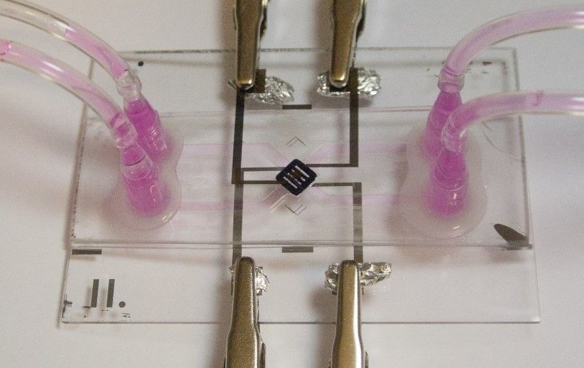
E1 E3

 E2 E4

Figure 4.4: Picture taken during impedance measurements. The electrode
annotations E1, E2, E3 and E4 was used during the measurements, as well as in
the data analysis and presentation.

 22
5. Results
The results obtained during the project consist of: observations from the literature
study; two electrode designs (square- and ring electrodes); fabricated electrodes
of silver or platinum on glass wafers; and impedance data for electrode testing.
The experimental results from the square electrodes and the ring electrodes are
presented separately, in different subsections of this chapter, but with a brief
comparison of their measurement reproducibility in the end of section 5.4.2.

5.1 Literature study
From the literature study, some important points were brought into consideration.
Firstly, a simple method to measure TEER from electrodes placed in the
microfluidic channels has been presented by van der Helm et al. [20]. By using
four electrodes, two on each side of the membrane, they demonstrate a technique
to directly isolate TEER from the system by combining measurements from the
four electrodes, without having to perform equivalent circuit modelling. The high
resistance from the microfluidic channels, and the associated measurement
variations, are directly cancelled out by the model. The model was thus shown to
reduce measurement related variations. Their methodology is to measure the
impedance between two electrodes for all electrode combinations, a total of six
measurements. The impedance values at 10 kHz are then extracted from the
impedance spectra and used for the calculation. The measured resistance between
two electrodes can be thought of as the sum of the resistances in its path, illustrated
in figure 5.1. As there are five unknown resistances and six measurements,
Gaussian elimination can then be applied to calculate the individual resistances of
the channels, I1-I4, and the resistance over the membrane and cellular barrier, Im.
TEER is calculated by formula 4, where A is the cell culture area and Ii-j is the
impedance from resistor i to resistor j. TEER is thus directly derived from the
resistance Im. The TEER of the system, measured prior to cell seeding, is
subtracted.

 1
 [Ω 2 ] = × (
 4 1→2
 + 1→4 + 2→3 + 3→4 − 2 1→3 −2 2→4 ) (4)

 23
Top channel

 Bottom channel

Figure 5.1: Schematic picture of the electrode configuration (adapted from van
der Helm et al. [20]). E1-E4 represent the electrodes, I1-I4 the channel resistances
and Im the resistance over the membrane.

Further, Odjik et al. [5] argue that the current over the cell culture area in a
microfluidic organ-on-chip may be unevenly distributed, which can result in a
faulty estimation of TEER. The uneven current distribution over the membrane
may be due to the geometry of the device or the configuration of the electrodes,
and can cause an uneven voltage drop, which gives a faulty estimation of the
membrane area. This may lead to an overestimation of TEER. The authors suggest
a mathematical model to correct for this effect.

Yeste et al. [31] also discuss this problem as a possible error contributing to the
large spread of variation of TEER measurements. From simulation studies on
models with different geometries and electrode configurations, they show that the
current distribution is dependent on the TEER value and the chamber height of
the microfluidic system. The most uniform field is found in systems with a
chamber height of 500 μm and larger and for TEER values larger than 103 Ωcm2.
The authors propose a formula including a geometric correction factor (GCF) to
account for a non-uniform sensitivity field. Further the authors point out placing
bipolar electrodes in the inlets and outlets of the system as a limiting factor unless
any correction is performed.

Booth et al. [18] suggest that electrodes should be placed directly over the
membrane, and cover at least 75% of the membrane area to assure that the
resistance measured is representative of the whole membrane. For other electrode
placements or electrode sizes, the current density field over the membrane should
be considered and accounted for. Van der Helm et al. [20] argues that a uniform
distribution across the barrier can be assumed in their model as the barrier
resistance is relatively larger than the local channel resistance at the membrane.

 24
TEER has commonly been presented normalised to surface area of the cell culture
membrane in the unit Ωcm2, for easy comparison to other models. A recent article
by Henry et al. [19] present TEER in the unit Ω without normalisation to cell
culture area, and question the biological significance of Ωcm2. They argue that the
unknown homogeneity of the field and instability in position of hand-manipulated
electrodes as well as the influence of indeterminate regions of the cell culture
outside the membrane contribute to uncertainties in estimated normalisation area.
They also point out that although the cell capacitance is commonly modelled as a
capacitor in equivalent circuit models in electrophysiology, constant phase
elements (CPE) may be used instead for a better fit of data to the model.

5.2 Electrodes
The two electrode designs that were created are visualised on glass slides in a 3D-
drawing below (figure 5.2). The total width of the chip was increased from 25 mm
to 51 mm, to allow connection to the electrode pads on both sides.

A complete, functioning fabrication protocol of the electrodes on glass was
developed (Appendix A). The fabrication protocol was used for both silver and
platinum electrodes. Sputtering of platinum required a considerably higher energy
than sputtering of silver. The platinum deposition had to be divided into several
parts to not overheat the evaporator. Part of the platinum layer was sputtered, then
the system had to cool down before continuing until the desired thickness was
reached. It therefore took longer time to fabricate the platinum electrodes. Some
artefacts in the photoresist pattern around the tubing holes on the glass was
observed, but these did not affect the area of electrode structures and channels.
As the electrodes were fabricated from the same mask they could be replicated
with very high precision, with minimal variation in electrode geometry between
glass slides. As the chip-layers were manually assembled some variation in
alignment occurred in their relative placement. The silver electrodes were very
fragile and easily physically damaged and could be wiped off with a paper towel.
They were therefore difficult to handle and very often damaged during the
bonding process when assembling the device. A brownish layer was sometimes
formed on the surface of the silver electrodes during the oxygen plasma bonding
to PDMS. Oxidation of silver by the oxygen plasma can result in a reduced
conductivity.

 25
A.

 B.

Figure 5.2 Schematic drawing of how the electrodes looks patterned on glass -
(A) square electrodes and (B) ring electrodes.

5.3 Impedance measurements: square
electrodes
Impedance measurements on chips without cells incorporated were performed to
evaluate the performance of the electrodes. The square electrodes were fabricated
and tested first, and therefore this design was used for the basic performance tests.
Firstly a prototype device, consisting of two electrodes in a single channel was
constructed to test if the electrodes could detect a signal. After obtaining
satisfactory impedance spectra from the prototype device, impedance
measurements were performed on fully assembled chips with and without a

 26
membrane. The experiments aimed to evaluate the choice of material, sensitivity
of the electrodes and the reproducibility of the measurements. The sensitivity was
tested by measuring the impedance with fluids of different conductivity in the
system, and observe if the electrodes could detect a change in conductivity.
Measurement reproducibility was tested by reproducing the experiments over a
time period up to 10 days, and study the variation between measurements. Efforts
were then made to test if combining measurements from all four electrodes can
reduce measurement variations of this system.

5.3.1 Characterisation of electrodes in single-channel prototype
device

The single channel prototype device that was constructed consisted of one glass
layer with thin film electrodes in silver, one layer of PDMS with one channel and
a ticker top layer of PDMS (figure 5.3). Very little variation was observed between
the measurements (figure 5.4). However, the electrodes were consumed quickly
as the silver of the electrodes pads was scraped off when connecting the probes.
After four measurements the circuit path was broken and the electrodes could no
longer pick up a signal. The number of measurements was therefore limited by
damage to the electrode pads. Soldering wires directly to the electrode pads also
failed as the thin silver layer was completely oxidized in the process.

Figure 5.3: Impedance measurement of single-channel prototype device with
silver electrodes. Probes from the impedance analyser are clamped to the
electrode pads with aluminium foil for better conductivity. The channel was
emptied and refilled between all measurements.

 27
Figure 5.4: Absolute impedance and phase shift spectra derived from the
impedance data measured on the prototype device. The highest impedance
magnitude, around 1200 Ω, was observed at low frequencies, in the region where
the double layer capacitance of the electrodes dominates. The impedance then
flattens out in the mid-frequency region, around 10 kHz which is a typically
readout frequency for TEER. The phase shift is at a minimum in this region. In the
high-frequency range, the impedance magnitude and phase shift both fall rapidly.

 28
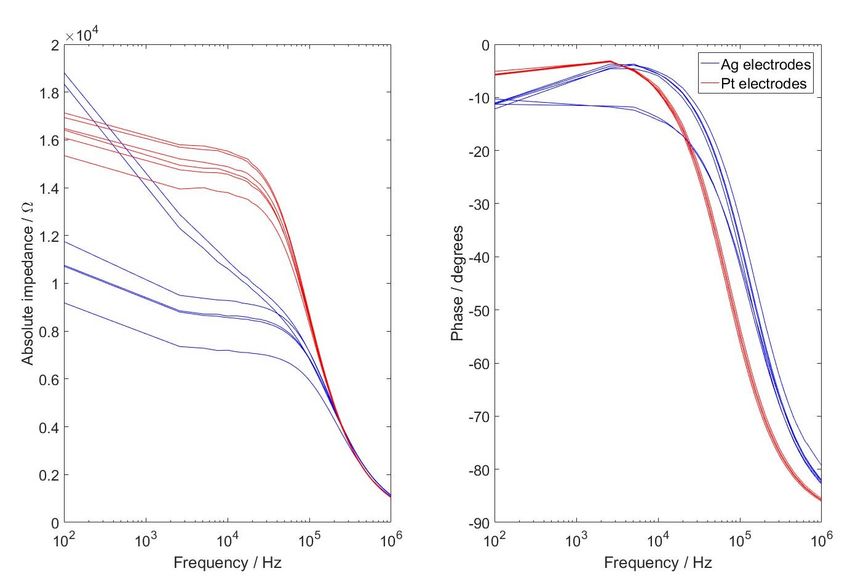
5.3.2 Silver electrodes vs. platinum electrodes

Impedance spectra measured with silver electrodes and platinum electrodes are
compared in figure 5.5. Measurements were performed on assembled chips
without membranes.

Figure 5.5: Impedance magnitude (left) and phase shift spectra (right) measured
on blank chips with platinum electrodes and silver electrodes. Six measurements,
one for each combination between the four electrodes, is shown for each chip.
Platinum electrodes measured a higher impedance magnitude than the silver
electrodes, but with less dispersion in the low- and mid-frequency range. Phase
shift spectra of the two metals were comparable.

Silver electrodes and platinum electrodes were both subjected to measurements
over 10 days under constant conditions. The silver electrodes failed to reproduce
the same spectra already after one measurement (figure 5.6), as the electrode pads
were damaged from the probes of the impedance analyser. The platinum
electrodes remained physically stable throughout the whole measurement period
of 10 days, (figure 5.7).

 29
Blank chip with silver electrodes, day 1

 A.

 Blank chip with silver electrodes, day 2

 B.

Figure 5.6: Impedance magnitude (left) and phase shift spectra (right) from a
blank chip with silver electrodes - (A) Day 1. (B) Day 2.
Dashed lines represent measurements across only one channel and solid lines
represent measurements from one channel to another, over the area where the
membrane is inserted.

 30
Blank chip with platinum electrodes, day 1

 Blank chip with platinum electrodes, day 5

 Blank chip with platinum electrodes, day 10

Figure 5.7. Impedance magnitude (left) and phase shift spectra (right) from a
blank chip with platinum electrodes - (A) Day 1. (B) Day 5. (C) Day 10.

 31
5.3.3 Characterisation of assembled chips

The impedance spectra from measurements on a fully assembled blank chip and a
chip with incorporated membrane measured with platinum electrode are presented
in figure 5.8. Some leakage was observed around the membrane of the chip with
membrane, which may have influenced the spectra.

 A.

 B.

Figure 5.8: Impedance magnitude (left) and phase shift spectra (right) from a (A)
blank chip with platinum electrodes and (B) chip with membrane with platinum
electrodes. The two chips have comparable impedance magnitudes, although the
chip with the membrane seems to have weakened the plateau effect in the mid-
frequency range. The chip with membrane also displays more phase shift in the
mid-frequency range. Interestingly, these properties were also observed in the
measurements between electrodes in the same channel that do not measure across
the membrane.

 32
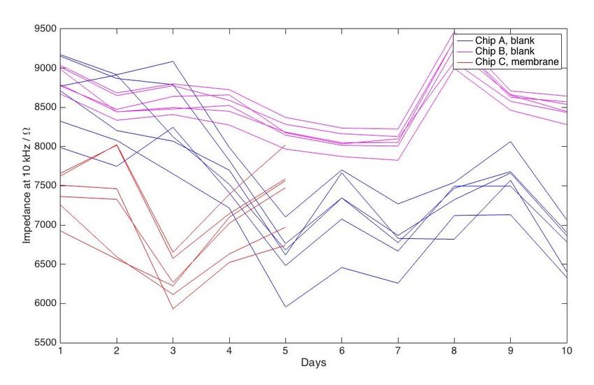
5.3.4 Sensitivity test

Tests performed with NaCl and diluted medium show that the electrodes are
sensitive to a change in electrolyte conductivity (figure 5.9). The medium was
estimated to have a conductivity close to 100 mM NaCl, which agrees with the
results obtained.

Figure 5.9: Impedance magnitude measured on a blank chip with platinum
electrodes, filled with different electrolyte of varying conductivity. A low
conductivity results in higher impedance.

5.3.5 Reproducibility test

Measurements on two blank chips were performed daily under constant conditions
over 10 days to observe the reproducibility of the measurements. The impedance
value at 10 kHz has been extracted from all measurements and is presented in
figure 5.10, to illustrate the measurement variations. The figure also shows the
same measurements performed on a chip with membrane, Chip C, over 5 days.
Chip A had some small parts of incomplete bonding between the top glass and
PDMS-layer. Chip B was assembled when the bonding protocol had been
optimised. Large measurements variations between days were observed for all
chips, especially for Chip A and Chip C which had not bonded completely.

 33
Figure 5.10: Impedance at 10 kHz measured over 10 days for two blank chips,
Chip A and Chip B, and one chip with membrane, Chip C. The graph shows the
measured impedance for all electrode combinations.

A protocol of combining measurements from the four electrodes, based on the
article by van der Helm et al. [20], was created attempting to isolate the impedance
over the cell membrane, Im, from which TEER can be directly calculated. Figure
5.11 presents the derived Im, isolated from the impedance of the channels.
Although there is still some variation, Im has much less variation than the
measured impedances in figure 5.10 for all 3 chips.

 34
Figure 5.11: Impedance Im , derived from combining the measurements in Figure
5.10.

5.4 Impedance measurements: ring electrodes
After characterising the square electrodes, the ring electrodes were fabricated in
platinum and tested in the same way. As they are placed much closed to each other
than the square electrodes, the impedance measured between the ring electrodes
was hypothesised to be lower than the square electrodes. Ring electrodes were
only fabricated in platinum.

5.4.1 Characterisation of an assembled chips

Impedance spectra measured from the ring electrodes are presented in figure 5.12
A. As expected, the impedance measured from the ring electrodes is lower than
the impedance of the same system with the square electrodes.
Impedance spectra measured on a system with incorporated membrane is
presented in figure 5.12 B. When comparing the spectra from the blank chip and
the chip with membrane, there was no apparent difference as a result of the
membrane.

 35
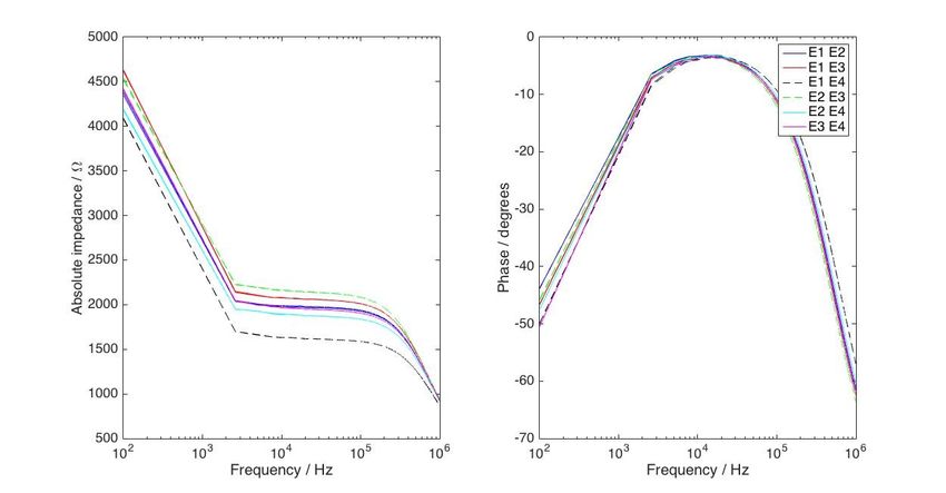
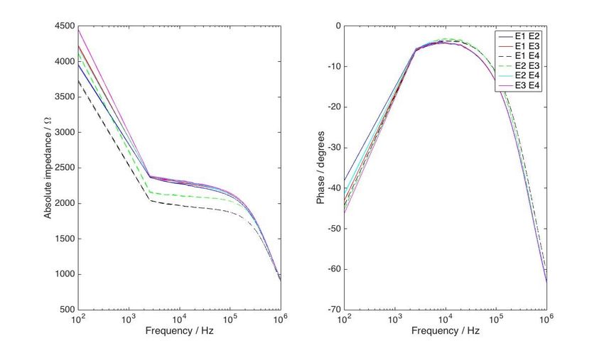
A.

 B.

Figure 5.12: Impedance magnitude (left) and phase shift spectra (right) from a
(A) blank chip with platinum ring electrodes and (B) chip with membrane with
platinum ring electrodes. In the mid-frequency range, a plateau at an impedance
of approximately 2 kΩ is formed. The smallest phase shift is observed around 10
kHz.

 36
5.4.2 Sensitivity test

The ring electrodes are also sensitive to a change in electrolyte conductivity
(figure 5.13). The medium had an impedance close 100 mM NaCl, as expected.

Figure 5.13: Impedance magnitude measured on a blank chip with platinum
electrodes, filled with different electrolytes of varying conductivity. A low
conductivity results in higher impedance.

5.4.3 Reproducibility test

The blank chip tested over 10 days, and found to produce stable spectra throughout
the measurement period. A chip with membrane was studied over 3 days. Like for
the square electrodes, the impedance at 10 kHz was extracted and plotted to study
measurement variations (figure 5.14). Some variation between measurements was
observed, but less than for the square electrodes.
Also, the same procedure of combining measurements to derive Im was performed
for the ring electrodes (figure 5.15). Im derived from combining measurements
was of similar magnitude as for the square electrodes. A reduction in variation
was also observed, however the difference was less significant than for the square
electrodes as the measurement from the ring electrodes showed much less
variation from the start.

 37
Figure 5.14: Impedance at 10 kHz measured over 10 days for a blank chip, and a
chip with membrane. The graph shows the measured impedance for all electrode
combinations.

Figure 5.15: Im, derived from combining the measurements in Figure 5.14.

 38
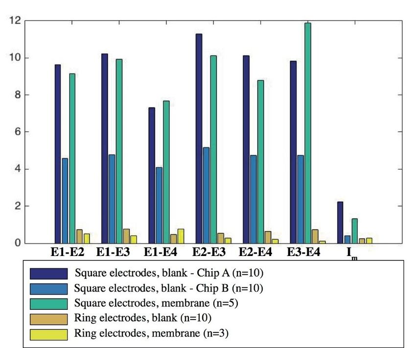
To further illustrate the difference in variation, standard error of mean (SEM)
values for were calculated for all measurements and their derived Im (figure 5.16).
SEM values were normalised to the membrane area for easy comparison to
reported uncertainly values of TEER in literature. SEM is proportional to the mean
value. Therefore, as the mean values of measured impedance from the square
electrodes are much larger than from the ring electrodes, in the range of 5-10 times
larger, there is no statistical relevance to comparing their SEM values.
However, Im is expected to be of the same magnitude for all chips. SEM values of
the calculated Im are lower for the ring electrodes, indicating less variation
compared to the square electrodes. Chip A and chip C which were observed to
leak, had SEM values between 1-2 Ωcm2, and the 3 remaining chips had SEM
values less than 0.5 Ωcm2. It can also be seen in the figure that SEM values of Im
are of similar magnitude as all measurements performed with the ring electrodes.

 Figure 5.16: Calculated SEM for all measurements and their derived Im,

 39
You can also read