A Versatile Hermetically Sealed Microelectronic Implant for Peripheral Nerve Stimulation Applications
←
→
Page content transcription
If your browser does not render page correctly, please read the page content below

ORIGINAL RESEARCH
                                                                                                                                              published: 22 July 2021
                                                                                                                                     doi: 10.3389/fnins.2021.681021

                                            A Versatile Hermetically Sealed
                                            Microelectronic Implant for
                                            Peripheral Nerve Stimulation
                                            Applications
                                            Dai Jiang 1 , Fangqi Liu 1 , Henry T. Lancashire 2 , Timothy A. Perkins 2 ,
                                            Matthew Schormans 1 , Anne Vanhoestenberghe 2,3 , Nicholas De N. Donaldson 2 and
                                            Andreas Demosthenous 1*
                                            1
                                             Department of Electronic and Electrical Engineering, University College London, London, United Kingdom, 2 Department of
                                            Medical Physics and Biomedical Engineering, University College London, London, United Kingdom, 3 Division of Surgery
                                            and Interventional Science, Aspire Centre for Rehabilitation Engineering and Assistive Technology, University College
                                            London, London, United Kingdom

                          Edited by:
               Morris (Ming-Dou) Ker,       This article presents a versatile neurostimulation platform featuring a fully implantable
       National Chiao Tung University,      multi-channel neural stimulator for chronic experimental studies with freely moving
                              Taiwan
                                            large animal models involving peripheral nerves. The implant is hermetically sealed
                        Reviewed by:
                           Aria Samiei,     in a ceramic enclosure and encapsulated in medical grade silicone rubber, and then
     University of Southern California,     underwent active tests at accelerated aging conditions at 100◦ C for 15 consecutive
                          United States
                                            days. The stimulator microelectronics are implemented in a 0.6-µm CMOS technology,
                            Yu-Wei Wu,
        Institute of Molecular Biology,     with a crosstalk reduction scheme to minimize cross-channel interference, and high-
              Academia Sinica, Taiwan       speed power and data telemetry for battery-less operation. A wearable transmitter
                              Jun Ohta,
              Nara Institute of Science     equipped with a Bluetooth Low Energy radio link, and a custom graphical user
      and Technology (NAIST), Japan         interface provide real-time, remotely controlled stimulation. Three parallel stimulators
                *Correspondence:            provide independent stimulation on three channels, where each stimulator supports
             Andreas Demosthenous
                                            six stimulating sites and two return sites through multiplexing, hence the implant can
          a.demosthenous@ucl.ac.uk
                                            facilitate stimulation at up to 36 different electrode pairs. The design of the electronics,
                   Specialty section:       method of hermetic packaging and electrical performance as well as in vitro testing with
         This article was submitted to
                    Neural Technology,
                                            electrodes in saline are presented.
               a section of the journal
                                            Keywords: hermetic seal package, implantable stimulator, microelectronics, power and data telemetry, wireless
            Frontiers in Neuroscience       stimulation control
           Received: 15 March 2021
            Accepted: 15 June 2021
            Published: 22 July 2021         INTRODUCTION
                             Citation:
        Jiang D, Liu F, Lancashire HT,      Direct interaction with neural pathways through active implantable devices has become an
            Perkins TA, Schormans M,        increasingly effective therapeutic approach for treating neurological disorders and organ defects,
                 Vanhoestenberghe A,        or replacing lost body function. Traditional clinical applications include cochlear implants for
                  Donaldson NDN and         hearing loss, deep brain stimulation (DBS) for epilepsy and Parkinson’s disease, and pacemakers
  Demosthenous A (2021) A Versatile
                                            for heart defects. More recent research includes epidural spinal cord stimulation for restoring
  Hermetically Sealed Microelectronic
          Implant for Peripheral Nerve
                                            coordinated locomotion in lower limbs (Capogrosso et al., 2016; Formento et al., 2018), peripheral
             Stimulation Applications.      nerve stimulation for creating tactile sensation after amputation (Raspopovic et al., 2014; Zollo
          Front. Neurosci. 15:681021.       et al., 2019), and vagus nerve stimulation for regulating organ function through neuromodulation
     doi: 10.3389/fnins.2021.681021         in order to reinstate a healthy balance (Famm et al., 2013; Pavlov and Tracey, 2017).

Frontiers in Neuroscience | www.frontiersin.org                                   1                                            July 2021 | Volume 15 | Article 681021
Jiang et al.                                                                                      Versatile Hermetically Sealed Microelectronic Implant

    Research on implantable active neural interface devices                The implant does not contain a built-in energy source. Power
require chronic studies in animal models in order to gain a                is supplied by the wearable transmitter over a wireless power
thorough understanding of the mechanism of neural diseases                 transfer link comprising two inductively coupled coils, which also
and disorders. Implantable devices used in these studies require           provides bidirectional half-duplex communication between the
accurate and highly selective neural stimulation at multiple               transmitter and the implant. The operation of the transmitter
sites. The stimulation should be highly programmable to                    is managed by a CC2640 microcontroller (MCU), which also
support closed-loop neural intervention. A variety of implantable          provides a Bluetooth Low Energy (BLE) radio link. This allows
stimulator designs has been reported in the literature in the past         the stimulation from the implant to be controlled from a
two decades. They can be divided into three major categories:              remote host computer. A custom BLE dongle was designed and
                                                                           fabricated for the radio link of the host computer, as shown in
   1) Implants adapted from commercially available devices
                                                                           Figure 1B. Dedicated software with a graphical user interface
      (Capogrosso et al., 2016; Boutros et al., 2019): Although
                                                                           (GUI) has been developed for wirelessly controlling the operation
      these implants have proven reliability, they are often
                                                                           of the implantable stimulator from the host computer. In
      limited by their inflexibility, coarse programmability, and
                                                                           experiments with free-moving animals, the wearable transmitter
      low channel count;
                                                                           could be mounted onto the animal subject in a jacket or
   2) Implants without hermetic packaging (Xu et al., 2015; Lee
                                                                           backpack, with the transmitter (Tx) coil in the inductive link
      et al., 2018; Williams et al., 2020): In these implants the
                                                                           aligned to the implanted receiver (Rx) coil. Researchers can
      electronics are encapsulated in silicone rubber or epoxy.
                                                                           set stimulation parameters on-the-fly from the GUI, where the
      This is a widely adopted approach because of its simple
                                                                           setting commands are transmitted via an USB-UART interface
      process and low cost. These devices, however, are often
                                                                           on the BLE dongle, then over the BLE link to the wearable
      used only in short-term animal studies due to the lack of
                                                                           transmitter, where the commands are relayed to the implant via
      adequate hermetic protection;
                                                                           the inductive link. This arrangement allows real-time control of
   3) In-house made prototype chronic implants: Some of these
                                                                           neurostimulation by the implantable stimulator without the need
      devices are packaged in precious metals (Hart et al., 2011;
                                                                           to attach a cable to the animal subject.
      Sun and Morrell, 2014; Zamora et al., 2020) and are
                                                                               The architecture of the wireless multi-channel stimulator
      expensive for production. Others are simple electronic
                                                                           system is shown in Figure 1A. The wearable transmitter
      circuits sealed in miniaturized glass packages (Loeb et al.,
                                                                           comprises a rechargeable battery, power management modules,
      2001; Sivaji et al., 2019), where the channel count and
                                                                           a class-D driver for driving the inductive link, wireless
      programmability are limited.
                                                                           communication modules and a MCU. The implantable
   This article presents the design, implementation, and                   stimulator has three parallel stimulators. The primary stimulator
evaluation of a versatile fully implantable multi-channel                  facilitates communication and manages the stimulation
stimulator implant for chronic animal studies targeting the                settings on all the three stimulators. It has a current pulse
peripheral nervous system. The implant is hermetically packaged            generator providing biphasic current pulses up to 1 mA,
in a ceramic enclosure and is cost effective as a research platform.       which are multiplexed to six stimulating electrodes and two
Inductive wireless powering removes the need for an implanted              return electrodes, supporting up to 12 different electrode
battery, avoiding potential battery failure. A bidirectional, high-        configurations. The primary stimulator control unit has
speed communication channel facilitates real-time programming              three parallel finite-state machines (FSMs) for managing the
of the implant from a remote external host computer allowing               stimulation settings on each stimulator. The FSMs for the two
free movement of the animal. Results from accelerated aging                secondary stimulators trigger the local secondary stimulation
tests at 100◦ C for 15 consecutive days demonstrate that the               control units to operate the current pulse generators, where
implantable stimulator is suitable for chronic implantation.               the current amplitude is amplified by a current booster to up
   The rest of the paper is organized as follows. Section “Materials       to 3 mA. Each secondary stimulator also supports up to 12
and Methods” describes the design and fabrication of the                   electrode configurations. Therefore, the implant can provide
hardware system, and the operation procedure for remote real-              three independent channels of parallel current stimulation for up
time stimulation control. Section “Results” show the electrical            to 36 different electrode pairs.
performance of the device as well as its suitability for chronic               As shown in Figure 1B, the implantable stimulator comprises
implantation. Section “Discussion and Conclusion” elaborates               a hybrid unit, where the stimulation electronics are mounted
on the findings and provides concluding remarks and future                 and sealed inside a ceramic package, a Rx coil printed circuit
directions.                                                                board (PCB) with a solenoid coil and tuning capacitors
                                                                           for inductive coupling, and three miniature connectors for
                                                                           connecting electrode arrays. The Rx coil PCB also has a
MATERIALS AND METHODS                                                      neodymium rare earth magnet (8 mm × 3 mm, Duratool) to
                                                                           aid alignment with the Tx coil PCB outside the body, which
System Architecture                                                        also has a magnet, as shown in Figure 1C. The optimal working
The wireless multi-channel stimulator system consists of a                 distance between the Tx and Rx coils is ∼ 1 cm. The hybrid,
hermetically sealed, fully implantable stimulator, as shown in             Rx coil PCB and connectors are joined with Cooner wires. The
Figure 1C, and a wearable transmitter, as shown in Figure 1B.              length between the hybrid and the Rx coil PCB is ∼ 55 mm, and

Frontiers in Neuroscience | www.frontiersin.org                        2                                        July 2021 | Volume 15 | Article 681021
Jiang et al.                                                                                                       Versatile Hermetically Sealed Microelectronic Implant

  FIGURE 1 | Wireless, fully implantable multi-channel stimulator: (A) System architecture; (B) Implantable stimulator; (C) Wearable transmitter and BLE dongle.

between the hybrid and the connectors is up to 180 mm. This                            silicone encapsulation ensure the suitability of the stimulator for
arrangement allows the Rx coil PCB to be implanted close to                            chronic implantation.
the skin for strong coupling, whilst the hybrid can be implanted
in a relatively deeper, surgically suitable location. In addition,                     Stimulator Circuits
the implantable electrode connectors provide the flexibility                           The circuits of the three stimulators are integrated onto three
of having the electrode cable at any desired length required                           application specific integrated circuits (ASICs) using a high-
to reach the targeted nerve. All the units are encapsulated                            voltage (HV) 0.6 µm CMOS technology. Figures 2A,B show
in medical grade silicone rubber. The hermetic package and                             the microphotographs of the primary and secondary stimulator

Frontiers in Neuroscience | www.frontiersin.org                                    3                                             July 2021 | Volume 15 | Article 681021
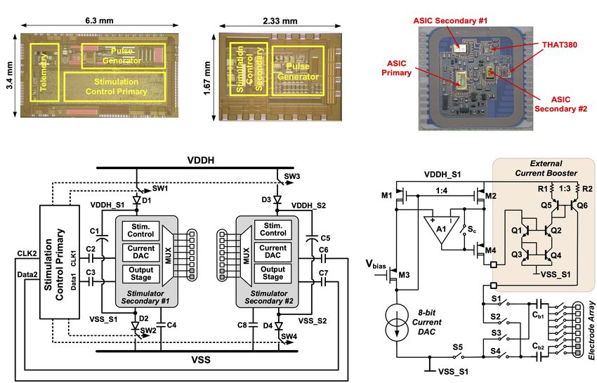
Jiang et al.                                                                                                        Versatile Hermetically Sealed Microelectronic Implant

  FIGURE 2 | Stimulator circuits: (A) Microphotograph of the primary stimulator ASIC; (B) Microphotograph of the secondary stimulator ASIC; (C) Layout of the
  stimulator circuits inside the hybrid; (D) Schematic of the power isolation scheme for crosstalk reduction; (E) Integrated pulse generator on Stimulator Secondary #1
  (the circuits for the integrated pulse generator on Stimulator Secondary #2 are identical).

ASICs, respectively. Bare dies of the stimulator ASICs, as                              #1 ASIC from the other stimulators. This isolation prevents
well as two commercially available THAT380 ICs, are wire-                               a potential current path from the stimulating electrodes to
bonded directly to printed pads inside the hermetically sealed                          electrodes connected to other stimulators and minimizes inter-
hybrid as shown in Figure 2C. In a conventional multi-channel                           channel electrical crosstalk. During isolation, the secondary ASIC
stimulator design, channel interference is addressed by either                          is supplied by the energy storage capacitor, C1. At the completion
interleaving the pulses from multiple channels (Zeng et al.,                            of the biphasic pulse, SW1 and SW2 are turned on again to
2008), or physically isolating the electrodes (Wong et al., 2007).                      recharge C1 until the next biphasic pulse. SW1 and SW2 are
The former approach correlates the channels hence reduces the                           implemented in the primary ASIC with complementary HV
degree of stimulation independence, while the latter approach                           MOSFETs. When Secondary #1 ASIC is isolated, the voltage at the
increases the size of the electrode array, which may be limited by                      negative terminal of C1, VSS_S1, may be lower than the substrate
surgical constraints. To ensure truly multi-channel stimulation,                        voltage of the primary ASIC at VSS. To ensure the NMOS in SW2
the implant uses a novel power isolation scheme (Jiang et al.,                          remains off, a diode D2 is added in series with SW2. Similarly, the
2015). Figure 2D shows the circuit arrangement for this scheme.                         voltage at the positive terminal of C1, VDDH_S1, may be higher
The two secondary stimulator ASICs are supplied from the 16 V                           than VDDH, which is the bias voltage of the NWELL for the
supply rails VDDH and VSS through a switched connection,                                PMOS in SW1. Diode D1 in series with SW1 ensures the PMOS
where the switches are controlled by the primary stimulation                            in SW1 remains off. The storage capacitors C1 and C5 are 2.2 µF.
control logic. Before the onset of a biphasic pulse from a                              When supplying a biphasic pulse at 3 mA with an overall pulse
secondary stimulator, for example, Stimulator Secondary #1,                             width of 1 ms, the voltage drop across the storage capacitor is
the primary control logic sends the pulse amplitude setting to                          (3 mA × 1 ms)/2.2 µF = 1.36 V. The on resistance of SW1, SW2,
the secondary stimulation control logic via ac coupled data                             SW3, and SW4 is 28  each, and the RC time constant when
connections CLK1 and Data1, so that the secondary logic can                             recharging the storage capacitors is 123.3 µs. For the maximum
control the local pulse generator to generate a biphasic pulse at                       specified pulse frequency is 500 pulse per second (pps), this time
the specified amplitude. During the biphasic pulse, the primary                         constant is sufficiently fast for recharging the storage capacitors
logic switches off SW1 and SW2 to isolate the Secondary                                 during the pulse interval.

Frontiers in Neuroscience | www.frontiersin.org                                     4                                             July 2021 | Volume 15 | Article 681021

Jiang et al.                                                                                                     Versatile Hermetically Sealed Microelectronic Implant

    Figure 2E shows the circuits of the pulse generator in                            flowing into these electrodes. S3 and S4 stay on during the pulse
Stimulator Secondary #1. The pulse generator in each ASIC                             interval for removing any remaining charges on the electrodes
consists of an 8-bit binary-weighted current digital-to-analog                        due to mismatch or charge leakage.
converter (DAC) with a resolution of 1 µA, an output stage
with active feedback to amplify the DAC current by four times,                        Power and Data Telemetry
and a “H-bridge” formed by S1–S4 to shape the current into a                          The implantable stimulator is powered by and communicates to
stimulus biphasic pulse. The width of the cathodic phase and                          the wearable transmitter via a power and data telemetry over an
anodic phase are programmable so that the biphasic pulse can                          inductive link (Donaldson and Perkins, 1983; Schormans et al.,
be either symmetrical or asymmetrical with a longer anodic                            2018). The circuit arrangement of the power and data telemetry
phase at a lower current amplitude. This is specified by the                          is shown in Figure 3A. The inductive link comprises a 5-turn,
stimulation settings, which can be programmed from the remote                         32-mm diameter Tx coil and a 7-turn, 28-mm diameter Rx coil.
host computer. The anode node between S1 and S3 connects via                          Both coils are solenoids wound using 0.5 mm gauge enameled
a 1 µF blocking capacitor (Cb1 ) to a 1-to-6 multiplexer, and the                     copper magnet wires. The Tx coil, L1, is driven by a class-D
cathode node between S2 and S4 to a 1-to-2 multiplexer, also via a                    amplifier consisting of two NMOS transistors, M1 and M2, using
1 µF blocking capacitor (Cb2 ); thus, the stimulation is selectable                   discrete IRLML2030 N-channel power MOSFETs. M1 and M2 are
between 1 of 6 stimulating electrodes and 1 of 2 return electrodes.                   switches turning on and off at 9.6 MHz. Their gates are driven
In each secondary stimulator a 1:3 current booster outside the                        by the secondary sides, S1 and S2, of a toroidal transformer,
ASIC further increases the maximum stimulating current to                             in opposite polarity. The toroidal transformer arrangement
3 mA. As shown in Figure 2E the current booster is implemented                        ensures a non-overlap time between the switching on of M1 and
as a source-degenerated current mirror using a discrete matched                       M2 to avoid shoot through current. The primary side of the
transistor array (THAT380 IC). Between current pulses, the pulse                      toroidal transformer, P, is driven by a Xilinx XC2V256 complex
generator is connected to VDDH and VSS but switches S1, S2,                           programmable logic device (CPLD) through a buffer 74AC14.
Sc , and S5 are off to isolate the electrodes from VDDH and                           The supply voltage of the class-D amplifier is provided by a
VSS, preventing stimulating current from other stimulators from                       dc-dc converter LT1615 with a programmable feedback resistor

  FIGURE 3 | Stimulator circuits: (A) Schematic of the power and data telemetry; (B) Schematic of the integrated OOK demodulator; (C) Photo of the top side of the
  wearable transmitter; (D) Photo of the bottom side of the wearable transmitter.

Frontiers in Neuroscience | www.frontiersin.org                                   5                                            July 2021 | Volume 15 | Article 681021
Jiang et al.                                                                                                          Versatile Hermetically Sealed Microelectronic Implant

implemented with a potentiometer AD5220; thus, the transferred                           transmitter circuitry is located inside a wearable unit, as shown
power over the inductive link can be controlled by the MCU.                              in the photos in Figures 3C,D. In the implant, L2, C1–C3, and
The Rx coil, L2, is tuned at 9.6 MHz with capacitor C1. The                              D1–D4 are located on the Rx coil PCB, and the rest of the implant
voltage across coil L2 is rectified by the Schottky diode D2 and                         electronics are mounted on the hybrid which is hermetically
a 10 µF capacitor C2, and regulated by a high voltage regulator                          sealed with a ceramic lid.
(MIC5233) to a stable dc supply voltage VDDH of 16 V. There is
also a middle tap on L2, where the voltage is rectified by D3 and                        Implant Packaging and Encapsulation
C3 and then is regulated by a 5 V linear regulator in the primary                        The implantable hybrid was constructed from a 36 mm × 38 mm
ASIC to a 5 V supply for the low voltage circuits in the implant.                        ceramic substrate (96% alumina) with a thickness of 0.635 mm.
The wearable transmitter is supplied by a lithium polymer battery                        Two layers of tracks were screen printed in thick film gold (8844-
LP-443440 (3.7 V, 560 mAh). The battery can be recharged from                            G Au) of 8 ± 1 µm thickness, with solder pads in the top layer
a USB port, regulated by a power management IC (LTC4160).                                over-printed with thick film platinum-gold (5837-G PtAu) of
   The inductive link also functions as a bidirectional half-duplex                      12 ± 2 µm thickness. Thick film multilayer dielectric (4913-
communication channel. The downlink data stream consisting                               G) was over-printed between the layers and also on top of the
of control commands and stimulation parameters are sent to                               top layer, covering all tracks except for the solder pads. A seal
the implant using on-off keying (OOK) modulation. The uplink                             ring was formed by screen printing a platinum-gold layer; this
data from the implant are transmitted using passive phase-                               also created hermetic feedthroughs for dielectric covered tracks
shifted keying (PPSK) modulation (Jiang et al., 2017). During                            from the hybrid circuit. All discrete components were soldered
downlink data transfer, the MCU on the wearable transmitter                              to the hybrid and flux residue was cleaned by sequential washes
sends stimulation settings received from the host computer over                          in acetone, propan-2-ol (isopropanol), and de-ionized water with
the BLE radio to the CPLD via a serial peripheral interface (SPI).                       ultrasonication. The primary stimulator ASIC, two secondary
The data frames are shifted in series at 400 kb/s to control an                          ASICs and two THAT380 bare dies were wire-bonded to the
internal switch to turn on and off a 9.6 MHz output signal,                              substrate, as shown in Figure 2B, and covered with epoxy glob
which drives the class-D amplifier. On the Rx side, the data                             top (Ablestik 968-2), as shown in Figure 4A. The hybrid was
stream is recovered from the modulated carrier at the middle                             dried and sealed hermetically using a custom-made metallized
tap of L2, where the carrier is first rectified by D4, and then the                      ceramic lid (A473, Kyocera) of 32.13 mm × 28.55 mm size,
envelope is extracted by an integrated envelope detector (ENV)                           6.2 ± 0.5 mm height, and 3 mm thickness, soldered to the screen-
and a Schmitt trigger in the primary ASIC. The circuit of the                            printed seal ring while the assembly was placed on a hot plate at
integrated OOK demodulator is shown in Figure 3B. The uplink                             150◦ C. Figure 4B shows the hermetically sealed hybrid.
data transfer is implemented with an integrated PPSK modulator.                             The circular Rx coil PCB was constructed on an FR4 printed
A logic “1” transmitted shorts L2 using an integrated switch SW                          circuit board with a diameter of 34 mm, onto which were
when the voltage across L2 crosses zero from the negative value                          mounted discrete passive components in individual hermetic
and holds for 1.5 carrier cycles. As a result, a current surge is                        packages, the alignment magnet, and a coil of 0.5 mm gauge
caused in L1 and causes a transient voltage peak on the tuning                           enameled copper magnet wire. The PCB was constructed without
capacitors C4 and C5. The transient voltage on C5 is demodulated                         solder resist and silkscreen, and with exposed copper traces (no
through a passive envelope detector formed by D5, R3, and                                pad finish) to improve encapsulant adhesion.
C6, and then is filtered and amplified. The bitstream is then                               The hybrid and Rx coil PCB were joined with multistrand
extracted using a comparator. Details of the PPSK demodulation                           fluoropolymer insulated stainless steel Cooner Wire (AS632,
circuits are presented in Jiang et al. (2017). L1, C4, C5, D5, R3,                       Cooner Wire Company, Chatsworth, CA, United States), which
and C6 are mounted on the Tx coil PCB and the rest of the                                was also used for electrode connection cables. Connection wires

  FIGURE 4 | Implant fabrication and encapsulation: (A) Stimulator circuits assembled on a ceramic substrate with the bare dies covered in epoxy glob top;
  (B) Stimulation circuits hermetically sealed in a metallized ceramic lid; (C) 3D-printed mold for encapsulation: mold for the hybrid (top) and mold for the Rx coil PCB
  (bottom); (D) fully encapsulated implant with a £2 coin as reference for the size.

Frontiers in Neuroscience | www.frontiersin.org                                      6                                              July 2021 | Volume 15 | Article 681021
Jiang et al.                                                                                     Versatile Hermetically Sealed Microelectronic Implant

were threaded through 1 mm bore silicone rubber tubes and                 on-the-fly. The GUI controls the Bluetooth connection, implant
soldered to form implantable cables. Three electrode connection           connection, and stimulation parameter settings. The layout of
cables were formed, one for each parallel stimulator ASIC                 the GUI is shown in Figure 5A. The top panel “Serial Ports
with the associated two stimulation and six return lines.                 Control” controls the Bluetooth and implant connect/disconnect
Electrode cables were terminated with miniature connectors                functions, including selecting the COM port number and setting
(Nano 360 Plastic Circulars, NCS-11-DD, Omnetics Connector
               R
                                                                          the baud rate. The default baud rate is 9600 b/s. The middle
Corporation, Minneapolis, MN, United States).                             panel “Implant Control” sets the stimulation parameters, where
    The hermetically sealed, soldered hybrid and the Rx coil              the three identical setting tags, “Stimulator 1,” “Stimulator 2,”
PCB were cleaned by sequential washes in acetone, propan-                 and “Stimulator 3,” are provided for each stimulator ASIC. The
2-ol, de-ionized water, Leslie’s soup, and de-ionized water,              setting parameters for each stimulator ASIC include selection of
with each cleaning stage ultrasound assisted. Leslie’s soup is            the stimulating and return electrodes, the amplitude and width
a mixture of 0.5 wt% detergent (Teepol-L, Teepol Products,                of the biphasic current pulses, the delay between the cathodic
Kent, United Kingdom), and 25 wt% trisodium phosphate                     and anodic phases, the pulse rate, the shape of charge-balanced
(anhydrous, 13438, Alfa Aesar, Heysham, United Kingdom), in               biphasic pulses (symmetrical or asymmetrical), and the length
de-ionized water. Cleanliness before encapsulation is essential           of a pulse train. The lower panel “Status Monitor” displays the
for the survival of long-term implants (Vanhoestenberghe and              received stimulation parameters and the expected waveform of
Donaldson, 2013; Lonys et al., 2017; Kiele et al., 2020). Following       current pulses. In the example shown in Figure 5A, the setting
rinsing, the conductivity of the rinse solution was monitored to          parameters specify stimulation between electrodes E1 and E8
confirm adequate cleanliness.                                             on Stimulator ASIC Primary, with symmetrical biphasic current
    The cleaned implants are encapsulated in silicone rubber.             pulses with 80 µA (setting step size 4 µA) in amplitude, 10 µs
A low viscosity, two-part silicone adhesive (EPM-2420, Avantor-           width (setting step size 1 µs) and a pulse period of 1 ms [after
NuSil, Radnor, PA, United States) was used to reduce the risk             reverse exponential conversion (Jiang et al., 2011)]. The expected
of voids and bubbles. EPM-2420 is mixed in a 1:1, Part A:                 waveform is shown in the Status Monitor.
Part B ratio using a speed mixer for 2 min at 2500 rpm (Dual
Asymmetric Centrifugal Laboratory Mixer System, DAC 150                   Control Procedure
FVZ-K, Synergy Devices Ltd). Two molds were designed in                   The backend software communicates with the wearable
Autodesk Inventor Fusion 2013 for the hybrid and Rx coil PCB.             transmitter via a BLE radio link, relayed by the BLE dongle. The
The molds were 3D printed in Verowhite Plus plastic with                  communication facilitates four different procedures: establishing
its gloss finish, to 0.1 mm precision, as shown in Figure 4C.             connection, sending stimulation parameters, reset implant, and
Companion “Dural” plates were machined so the mold halves                 terminating connection, as shown in Figure 5B (the operations
could be bolted together. Implants were held in the cleaned molds         in the light boxes are executed by the host computer and
using pre-formed silicone spacers. Implants were encapsulated             those in the shaded boxes by the MCU module CC2640 on the
under vacuum (60 mBar) in a centrifuge (up to 200 g) to                   wearable transmitter).
remove air bubbles. Because of the 65◦ C temperature limit of                 The overall communication procedure between the GUI and
the Verowhite mold, the silicone rubber was cured at 60◦ C for            the implant for controlling multi-channel stimulation is shown in
4 h. The implants were extracted from the mold, and sections              Figure 5C. During the “establishing connection” procedure, the
of Dacron reinforced silicone rubber sheet were glued to the              link between the implant and the wearable transmitter, and the
encapsulated implant with EPM-2420 to create suture sites for             link between the wearable transmitter and the PC, are established
surgery. Free from the molds, the silicone rubber was further             separately. After the implant is powered, it sends a handshake
cured for 1 h at 80◦ C to complete the encapsulation. The                 request to the wearable transmitter via the inductive link every
encapsulated implant is shown in Figure 4D. An alternative                250 µs until it receives confirmation from the transmitter, after
medical grade silicone (MED-6215, Avantor-NuSil) is under                 which communication over the inductive link is established. The
investigation for long-term implantable devices.                          communication between the PC and the wearable transmitter
    Cleaned miniature connectors are also encapsulated                    is established after a “connecting” request is sent from the
in silicone rubber (Lancashire et al., 2021). Silicone tubing             GUI with a specified baud rate and serial port number, where
was placed at the base of each connector, surrounding the                 the host computer then wakes up the BLE dongle to establish
soldered wire ends. EPM-2420 silicone was degassed at 30 mbar             Bluetooth connection with the wearable transmitter. The MCU
in a vacuum centrifuge for between 1 and 3 min, until bubbles             on the wearable transmitter classifies the received command
were no longer visible, nor flew onto the wire ends, covering all         and sends a confirmation back to the host computer, hence the
exposed solder. Silicone was cured at 80◦ C for 3 h under pressure        communication between the host computer and the implant is
(2.5 bar) to shrink any bubbles present.                                  established, as shown in Figure 5B.
                                                                              Stimulation from the implant can be controlled from the PC
                                                                          following the “setting parameters” procedure, where stimulation
Stimulation Control Procedure                                             parameters set in the GUI are sent in packets via the Bluetooth
Graphical User Interface                                                  link to the transmitter, which repackages the data into frames
A GUI was developed in Matlab R2020a (MathWorks, Natick,                  shown in Figure 5D and forward the frames to the implant
MA, United States) for remotely controlling the stimulation               over the inductive link. The implant verifies the received setting

Frontiers in Neuroscience | www.frontiersin.org                       7                                        July 2021 | Volume 15 | Article 681021
Jiang et al. Versatile Hermetically Sealed Microelectronic Implant FIGURE 5 | Stimulation control protocol: (A) Graphical user interface; (B) Four procedures for operating the implant from a host computer, with flowcharts on the wearable transmitter in each procedure; (C) Overall communication procedure between the host computer and the implant for establishing connection and setting stimulation parameters; (D) Structure of the data frames over the inductive link; (E) Block diagram of the stimulation control logic in the implant, with an example of changing stimulation parameters on-the-fly. parameters using cyclic redundancy check (CRC) in the frames, for continuously generating stimulation pulses as specified, and sends back an acknowledgment frame to the transmitter as illustrated in Figure 5E (Jiang et al., 2011). Figure 5E with indicating whether the parameters are correctly received illustrates the change in stimulation pulses by the two “setting or a resend is needed. When all parameters are correctly parameters” procedures. received, the wearable transmitter sends confirmation back The operation of the implant can be reset by the “reset to the host computer to complete the “setting parameters” implant” procedure. When reset is requested from the GUI to procedure. This procedure is repeated when changes to the the transmitter, as shown in Figure 5B, the transmitter will stimulation are needed. After each procedure, the stimulation temporarily terminate the power delivery to the implant, which control logic in the primary stimulator ASIC stores the settings forces the implant to conduct a power-on reset. This safety feature in a built-in memory, where the state-machine for the selected provides an emergency exit to terminate stimulation from the stimulator repeatedly loads the parameters from the memory implant during experiments. After an experiment session, the Frontiers in Neuroscience | www.frontiersin.org 8 July 2021 | Volume 15 | Article 681021
Jiang et al.                                                                                                            Versatile Hermetically Sealed Microelectronic Implant

Bluetooth link between the PC and the transmitter can be released                         to water vapor, the most likely failure mode is driven by
by the “terminate connection” procedure, as shown in Figure 5B.                           the penetration of moisture through the encapsulation layer
                                                                                          (Donaldson, 1996). Should there be any ionic contamination
                                                                                          on the implant surface (underneath the silicone encapsulation
RESULTS                                                                                   layer), then the osmotic gradient driving water molecules toward
                                                                                          the contaminant and contributing to forming a pocket of
The performance of the fully implantable stimulator was                                   liquid water, is worse in deionized water than in saline, further
evaluated by electrical and in vitro experiments with electrodes                          accelerating the failure rate. Therefore, for an implant of this type
in saline, and by accelerated lifetime testing.                                           fully encapsulated in silicone, long-term tests in deionized water
                                                                                          are appropriate. The flask was continuously heated on a heating
Feasibility for Chronic Implantation                                                      mantle (Thermo Fisher Scientific, Waltham, MA, United States)
The quality of the seal of the implantable hybrid was tested                              at the boiling temperature for 15 consecutive days. A reflux
according to the MIL-STD-883 (MIL-STD-883L, 2019) standard                                condenser was installed on the flask to keep the volume of the de-
test for hermeticity. After sealing the lid, the package was bombed                       ionized water unchanged. The implant was inductively powered
in helium for 2 h at 2 bars, then transferred (maximum delay                              by the first version of the wearable transmitter (Jiang et al., 2016)
1 h) to a mass spectrometer for a fine leak test. The test was                            continuously during the entire course of the accelerated lifetime
considered passed if the leak rate was lower than 5 × 10⁻⁸ atm                            test. Data packets from the implant were frequently checked
cc/sec helium. After passing this fine leak test, the hybrid was                          to monitor the status of the implant electronics and to ensure
placed in gross leak tank at 125◦ C for 1 min, and the package                            the wireless power transfer at a level sufficient for operation.
was considered to be sufficiently hermetic if no bubbles were                             Figure 6B shows the Rx coil PCB before the accelerated lifetime
observed. Following this procedure, for hybrids that pass the                             test, and Figure 6C shows the Rx coil PCB immediately after the
tests, the minimum time for the internal humidity was estimated                           implant was extracted from the flask at the end of the 15-day test.
to reach 60% RH to be at least 151 days, or 47 days minimum                               No corrosion was observed.
to reach 30% RH. Note that the actual times are likely to                                    After returning to room temperature, the implant was placed
be much longer because the actual leak rate is likely to be                               in de-ionized water at room temperature but with the top surface
much lower, but the exact leak rates is not available as the                              exposed to open air. The implant was inductively coupled with
MIL-STD-883 standard only specifies a pass/fail fine leak test                            the wearable transmitter and the three stimulators were set to
(Vanhoestenberghe and Donaldson, 2011).                                                   generate current pulses at the maximum amplitude at 500 pps.
   The suitability of the implantable stimulator for chronic                              Immediately after the stimulation starts, a thermal image was
implantation was evaluated by accelerated lifetime testing. The                           taken using a FLIR E4 thermal imaging camera (FLIR Systems,
test setup is shown in Figure 6A. The implant was placed inside a                         Wilsonville, OR, United States). The surface temperature was
round bottom flask filled with de-ionized water. Deionized water                          25.5◦ C, as shown in Figure 6D. The implant was allowed to
was used to reduce the challenge of evaporation changing saline                           continuously operate for 1 h at the same settings, then the surface
concentration. The silicone rubber used has low permeability                              temperature was measured again, which increased to 26.7◦ C, as
to metal salts (Donaldson et al., 2011) and high permeability                             shown in Figure 6E.

  FIGURE 6 | Evaluation of feasibility for chronic implantation. (A) Setup of accelerated lifetime test; (B) Photo of the Rx coil PCB before the accelerated lifetime test;
  (C) Photo of the Rx coil PCB after accelerated lifetime test for 15 days; (D) Thermal image of the implant immediately after switched on at room temperature;
  (E) Thermal image of the implant 1 h after switched on in room temperature.

Frontiers in Neuroscience | www.frontiersin.org                                       9                                               July 2021 | Volume 15 | Article 681021
Jiang et al. Versatile Hermetically Sealed Microelectronic Implant
Electrical Performance Evaluation number. All stimulators were set to generate symmetrical
The electrical performance of the implantable stimulator was biphasic pulses with a pulse width of 200 µs. Pulses on the
evaluated with in vitro experiments both before and after the primary stimulator were at a constant pulse rate of 100 pps but
accelerated lifetime test. No changes were observed. Figure 7 the amplitude was modulated sinusoidally at 4.5 Hz between
illustrates the setup of the in vitro experiments, where the 250 µA and 1 mA. Pulses on Stimulator Secondary #1 were at
implant was submerged in saline solution (16.7 mS/cm2 ) and was a constant amplitude of 800 µA but the pulse rate was modulated
inductively coupled with the wearable transmitter. An epidural sinusoidally at 4.5 Hz between 400 pps and 53 pps. Pulses on
electrode array (Courtesy of Fraunhofer IMM) (Capogrosso et al., Stimulator Secondary #2 were modulated both in frequency and
2016) was connected to the implant and was also submerged amplitude, where the frequency modulation was the same as
in saline solution. There are 15 gold electrodes in a size of that on Stimulator Secondary #1, and the amplitude modulation
1.8 mm × 1 mm on a polyimide substrate distributed to the three was a 2-level step change between 700 µA and 1 mA, also at
stimulators. Sensing resistors were connected in series with the 4.5 Hz. Figure 8B demonstrates multiplexing stimulation among
electrode array for measuring the current pulses using a DSO- electrode pairs on the primary stimulator. In the first 300 ms,
X 2024A oscilloscope (Keysight, Santa Rosa, CA, United States). stimulation was from electrodes E1 and E8, with a current
Stimulation was set from the GUI on a remote host computer. amplitude of 800 µA at a pulse rate of 100 pps. From 300 ms
Note that the epidural electrode array was not included in the to 400 ms, the pulse rate was increased to 200 pps, and the pulses
accelerated lifetime test. were multiplexed between E1 and E2 at a fixed interval of 5 ms,
The results shown in Figures 8A–C, 9 were recorded after the as highlighted in the zoom-in view, effectively providing 100 pps
accelerated lifetime test. Figure 8A shows parallel stimulation stimulation at both E1 and E2. After 400 ms, the pulse rate was
from the three stimulators. The modulation patterns in this changed back to 100 pps and stimulation was from E2 only. This
test were prestored in the CPLD on the wearable transmitter, process repeated after 500 ms between E2 and E3. The tests shown
where the remote host selected the patterns by their identification in Figures 8A,B were repeated for all the 36 electrode pairs.
FIGURE 7 | Diagram of the in vitro benchtop performance evaluation setup. Insert: photo of the wearable transmitter and implantable stimulator during the in vitro
experiment.
Frontiers in Neuroscience | www.frontiersin.org 10 July 2021 | Volume 15 | Article 681021Jiang et al. Versatile Hermetically Sealed Microelectronic Implant
FIGURE 8 | In vitro electrical performance evaluation: (A) Parallel stimulation on the three stimulators in different modes of modulation; (B) Pulses multiplexed among
electrodes on the primary stimulator; (C) Concurrent stimulating pulses from the two secondary stimulators with minimized crosstalk; (D) Concurrent stimulating
pulses from a benchtop setup with the same circuits but without the power-isolation scheme.
Figure 8C shows the two secondary stimulators delivering performance, a benchtop stimulator using the same stimulator
concurrent biphasic pulses to the electrode array in saline ASICs in the same circuit arrangement was tested in the same
solution (16.7 mS/cm2 ). The pulses from Stimulator Secondary setup, but the two secondary stimulator ASICs are constantly
#1 are symmetrical, and the pulses from Stimulator Secondary connected to the power rails without isolation. The measured
#2 have anodic phases 8 times longer in width than the cathodic pulses are shown in Figure 8D. Significant distortion can be
phases, and 8 times lower in amplitude to retain charge balance. observed on pulses from both stimulators when they occur at
Minimal spikes can be seen on the pulses from Stimulator the same time. As shown in Figure 2E, the stimulating current
Secondary #2 when they occur at the same time as the pulses from between an electrode pair is generated from the current source
Stimulator Secondary #1. To compare the crosstalk reduction and passes through the electrode pair via the H-bridge formed
by S1 – S4 toward VSS_S1. When current pulses on both the
stimulators occur at the same time, if VDDH_S1 and VDDH_S2,
as well as VSS_S1 and VSS_S2, are shorted, part of the stimulating
current on Stimulator Secondary #2 finds a pathway to VSS_S1
via the stimulating electrode pair on Stimulator Secondary #1,
resulting in the distortion on the current pulses, as shown on
the last two pulses in Figure 8D which are measured on the
stimulators on the current path from the electrode pair to VSS_S1
(or VSS_S2), as shown in Figure 7. The first two biphasic pulses
on Stimulator Secondary #2 in Figure 8D occur in the pulse
interval on Stimulator Secondary #1, while S1, S2, and S5 in
Stimulator Secondary #1 are off, as the crosstalk current pathway
does not exist and the measured pulses are intact.
FIGURE 9 | Measured carrier waveform on the Tx tuning capacitor showing The charge balancing performance of the stimulators was
both OOK and PPSK modulation, alongside the measured downlink bitstream. evaluated using the test setup shown in Figure 7, where the dc
Frontiers in Neuroscience | www.frontiersin.org 11 July 2021 | Volume 15 | Article 681021Jiang et al. Versatile Hermetically Sealed Microelectronic Implant
voltage across the sensing resistor was measured after a second- TABLE 1 | Features and performance of the implant system.
order low-pass filter with a cut-off frequency of 0.28 Hz. The Hybrid dimensions 46 mm × 42.8 mm × 8.8 mm
stimulator under test was set to generate biphasic pulses at Weight 35.2 g
500 pps, with a current amplitude of 1 mA and a pulse width Packaging Hermetically sealed ceramic package with silicone
of 100 µs per phase. The stimulation operated continuously encapsulation
for 8 h, and the dc voltage across a 790 sensing resistor Stimulator ASICs 0.6-µm HV CMOS
was measured every 30 min. The measured voltage remained Supply voltage 5 V (digital circuits), 16 V (stimulator output stage)
constant at ∼ 1 µV, suggesting a residue dc current of ∼ 1.27 nA. Implant supply Wireless inductive powering
Wearable transmitter Rechargeable 3.7 V battery
There are various safety limits for neurostimulation reported in
supply
literature on the residue dc current, for example, 25 nA (Sit Power consumption 31 mW*
and Sarpeshkar, 2007) and 100 nA (Huang et al., 1999). The (stimulators)
actual safety threshold should be placed in context with the Stimulation type Biphasic constant current pulsatile stimulation
equivalent charge density and the location of the electrodes. Stimulation amplitude Primary ASIC: 8-bit current DAC, 0 µA – 1 mA, step size
Nevertheless, the measured dc current is much lower than 4 µA
Secondary ASICs: 8-bit current DAC, 0 µA – 3 mA, step
these safety limits. size 12 µA
Figure 9 shows the measured modulation on the carrier over Pulse rate 1–500 pps, resolution ≤0.5 pps
the inductive link for sending bitstreams in both directions. The Pulse duration Cathodic phase: 0–500 µs
upper waveform is the voltage measured at the input of the Anodic phase: 1–8 times cathodic width
envelope detector in the Tx coil PCB, i.e., the voltage across Number of stimulators 3, each driving 6 stimulating electrodes and 2 return
electrodes
capacitor C5 in Figure 3A, and the lower waveform is the control
Number of electrode 36
signal for the OOK modulation switch in the CPLD. It shows configurations
a carrier modulated first in OOK to send a 28-bit stimulation Inductive link Primary coil: 32 mm diameter, 0.5 mm gauge, 5 turns,
setting frame to the implant at 400 kb/s, and then is modulated parameters 1.85 µH Secondary coil: 28 mm diameter, 0.5 mm
in PPSK by the implant to send back a 11-bit acknowledgment gauge, 7 turns, 2.52 µH
frame at 600 kb/s. Inductive link working 3–11 mm
distance
A battery life test showed the voltage of a fully charged lithium
Received DC suppliedJiang et al. Versatile Hermetically Sealed Microelectronic Implant
The electrical performance evaluation demonstrates the the stimulator ASICs, and could be eliminated with a new
stimulator’s capability of providing versatile stimulation on stimulator ASIC design.
multiple channels under real-time remote control. More 3) Communication Latency: In the first version transmitter
importantly, it demonstrated that the implantable stimulator can design (Jiang et al., 2016), an easyRadio ISM module
provide truly parallel multichannel stimulation where current eRA900TRS was used for the communication with the
pulses on different channels can occur at the same time with remote host, chosen for its low power consumption, but it
minimal channel interference due to crosstalk. This feature was found that the inter packet delay is not optimal. A BLE
allows simultaneous, highly selective stimulation to multiple sites, radio link is chosen for the second version transmitter
especially with different stimulation patterns on each site. design. In the 9.4 ms communication latency, 8.3 ms is from
The implantable stimulator provides a versatile platform for the slow UART communication between the host computer
chronic experimental studies with freely moving animals for and the BLE dongle. This latency could easily be shortened
applications involving peripheral nerves, such as vagus nerve by selecting a higher UART baud rate.
stimulation, spinal cord injury and hand neural prostheses.
Stimulation for up to 36 different electrode pairs can be facilitated
and connections to the electrodes are “plug & play” allowing the DATA AVAILABILITY STATEMENT
use of different electrodes to suit each particular application.
Future work could consider the following enhancements in The original contributions presented in the study are included
the electronics: in the article/supplementary material, further inquiries can be
directed to the corresponding author/s.
1) Power Consumption: As the ASICs are implemented in
0.6 µm CMOS technology, the control logic and the low
voltage analog modules such as the 8-bit current DAC are
AUTHOR CONTRIBUTIONS
operating at a 5 V supply voltage. The power consumption DJ, FL, HL, TP, and AV drafted the manuscript. DJ, FL, and
of these modules is over 20 mW. Implementation in a MS developed the hardware and firmware. FL developed the
more advanced CMOS process technology (e.g., 180 nm graphical user interface. DJ, HL, TP, and AV conducted implant
HV CMOS), allows the supply voltage to the control logic, packaging and encapsulation. DJ, FL, MS, HL, TP, and AV
biasing circuits and the current DAC to be reduced to designed and conducted the benchtop device evaluation. ND
1.8 V or lower, reducing the power required. For example, and AD supervised the research and reviewed the manuscript.
the integrated stimulator presented in Jiang et al. (2021) All authors contributed to the article and approved the
is implemented 180 nm CMOS and consumes only 1 mW submitted version.
when generating 50 Hz, 50% duty cycle current pulses of
16 mA. The energy consumed by the output stage circuit
can be reduced by dynamic compliance voltage techniques FUNDING
(Samiei and Hashemi, 2021) and energy recycling methods
(Ha et al., 2019); This work was supported in part by the European Commission
2) Physical Size: The power isolation scheme requires the under projects NEUWalk and CLONS (agreement numbers
substrate of the parallel stimulators to be separated. 258654 and 225929). The open access publication fees were
Using 0.6 µm CMOS technology, the stimulators have to provided by University College London.
be implemented in separate ASICs. The use of silicon-
on-insulator (SOI) CMOS technology would allow a
single chip solution for all the stimulator circuits in ACKNOWLEDGMENTS
the implant. In addition, a high-frequency stimulation
scheme (Jiang and Demosthenous, 2018) allows on-chip The authors would like to thank Prof. David Borton from Brown
energy storage capacitors, which could further reduce University for the discussions on the device specifications and Dr.
the physical size of the circuit layout. Furthermore, the Peter Detemple from Fraunhofer IMM for providing the epidural
external current booster using THAT380 was external to electrode array for the in vitro evaluation.
REFERENCES BSI (2015). BS EN 45502-1:2015 Implants For Surgery—Active Implantable Medical
Devices Part 1: General Requirements For Safety, Marking And For Information
Au, S. L. C., Chen, F.-Y. B., Budgett, D. M., Malpas, S. C., Guild, S.-J., and to be Provided by the Manufacturer. London: BSI Standards Limited.
McCormick, D. (2020). Injection molded liquid crystal polymer package Capogrosso, M., Milekovic, T., Borton, D., Wagner, F., Moraud, E. M., Mignardot,
for chronic active implantable devices with application to an optogenetic J.-B., et al. (2016). A brain–spine interface alleviating gait deficits after spinal
stimulator. IEEE Trans. Biomed. Eng. 67, 1357–1365. doi: 10.1109/tbme.2019. cord injury in primates. Nature 539, 284–288. doi: 10.1038/nature20118
2936577 Dahan, N., Vanhoestenberghe, A., and Donaldson, N. (2012). Moisture ingress into
Boutros, P. J., Schoo, D. P., Rahman, M., Valentin, N. S., Chow, M. R., Ayiotis, packages with walls of varying thickness and/or properties: a simple calculation
A. I., et al. (2019). Continuous vestibular implant stimulation partially restores method. IEEE Trans. Compon. Packaging Manuf. Technol. 2, 1796–1801. doi:
eye-stabilizing reflexes. JCI Insight 4:e128397. doi: 10.1172/jci.insight.128397 10.1109/tcpmt.2012.2210425
Frontiers in Neuroscience | www.frontiersin.org 13 July 2021 | Volume 15 | Article 681021Jiang et al. Versatile Hermetically Sealed Microelectronic Implant
Donaldson, N. D., and Perkins, T. A. (1983). Analysis of resonant coupled coils in implantable gastrostimulator. Med. Biol. Eng. Comput. 53, 319–329. doi: 10.
the design of radio frequency transcutaneous links. Med. Biol. Eng. Comput. 21, 1007/s11517-014-1236-9
612–627. doi: 10.1007/bf02442388 MIL-STD-883L (2019). Test Method Standard Microcircuits. Columbus, Ohio:
Donaldson, N., Baviskar, P., Cunningham, J., and Wilson, D. (2011). The Department of Defence, USA.
permeability of silicone rubber to metal compounds: relevance to implanted Pavlov, V. A., and Tracey, K. J. (2017). Neural regulation of immunity: molecular
devices. J. Biomed. Mater. Res. A 100, 588–598. doi: 10.1002/jbm.a.33257 mechanisms and clinical translation. Nat. Neurosci. 20, 156–166. doi: 10.1038/
Donaldson, P. E. K. (1996). The essential role played by adhesion in the technology nn.4477
of neurological prostheses. Int. J. Adhes. Adhes. 16, 105–107. doi: 10.1016/0143- Raspopovic, S., Capogrosso, M., Petrini, F. M., Bonizzato, M., Rigosa, J., Pino,
7496(95)00031-3 G. D., et al. (2014). Restoring natural sensory feedback in real-time bidirectional
Famm, K., Litt, B., Tracey, K. J., Boyden, E. S., and Slaoui, M. (2013). A jump-start hand prostheses. Sci. Transl. Med. 6:222ra19. doi: 10.1126/scitranslmed.
for electroceuticals. Nature 496, 159–161. doi: 10.1038/496159a 3006820
Formento, E., Minassian, K., Wagner, F., Mignardot, J. B., Le Goff-Mignardot, Samiei, A., and Hashemi, H. (2021). Energy efficient neural stimulator with
C. G., Rowald, A., et al. (2018). Electrical spinal cord stimulation must preserve dynamic supply modulation. Electron. Lett. 57, 173–174. doi: 10.1049/ell2.
proprioception to enable locomotion in humans with spinal cord injury. Nat. 12024
Neurosci. 21, 1728–1741. doi: 10.1038/s41593-018-0262-6 Schormans, M., Valente, V., and Demosthenous, A. (2018). Practical inductive link
Ha, S., Kim, C., Park, J., Cauwenberghs, G., and Mercier, P. P. (2019). A design for biomedical wireless power transfer: a tutorial. IEEE Trans. Biomed.
fully integrated RF-powered energy-replenishing current-controlled stimulator. Circuits Syst. 12, 1112–1130. doi: 10.1109/tbcas.2018.2846020
IEEE Trans. Biomed. Circuits Syst. 13, 191-202. Sit, J.-J., and Sarpeshkar, R. (2007). A low-power blocking-capacitor-free charge-
Hart, R., Bhadra, N., Montague, F. W., Kilgore, K. L., and Peckham, P. H. balanced electrode-stimulator chip with less than 6 nA dc error for 1-mA
(2011). Design and testing of an advanced implantable neuroprosthesis with full-scale stimulation. IEEE Trans. Biomed. Circuits Syst. 1, 172–183. doi: 10.
myoelectric control. IEEE Trans. Neural Syst. Rehabil. Eng. 19, 45–53. doi: 1109/tbcas.2007.911631
10.1109/tnsre.2010.2079952 Sivaji, V., Grasse, D. W., Hays, S. A., Bucksot, J. E., Saini, R., Kilgard, M. P., et al.
Huang, C. Q., Shepherd, R. K., Carter, P. M., Seligman, P. M., and Tabor, B. (1999). (2019). ReStore: a wireless peripheral nerve stimulation system. J. Neurosci.
Electrical stimulation of the auditory nerve: direct current measurement in vivo. Methods 320, 26–36. doi: 10.1016/j.jneumeth.2019.02.010
IEEE Trans. Biomed. Eng. 46, 461–469. doi: 10.1109/10.752943 Sun, F. T., and Morrell, M. J. (2014). The RNS system: responsive cortical
Jiang, D., and Demosthenous, A. (2018). A multichannel high-frequency power- stimulation for the treatment of refractory partial epilepsy. Expert Rev. Med.
isolated neural stimulator with crosstalk reduction. IEEE Trans. Biomed. Devices 11, 563–572. doi: 10.1586/17434440.2014.947274
Circuits Syst. 12, 940–953. doi: 10.1109/tbcas.2018.2832541 Vanhoestenberghe, A., and Donaldson, N. (2011). The limits of hermeticity test
Jiang, D., Cirmirakis, D., and Demosthenous, A. (2015). A vestibular prosthesis methods for micropackages. Artif. Organs 35, 242–244. doi: 10.1111/j.1525-
with highly-isolated parallel multichannel stimulation. IEEE Trans. Biomed. 1594.2011.01222.x
Circuits Syst. 9, 124–137. doi: 10.1109/tbcas.2014.2323310 Vanhoestenberghe, A., and Donaldson, N. (2013). Corrosion of silicon integrated
Jiang, D., Cirmirakis, D., Schormans, M., Perkins, T. A., Donaldson, N., and circuits and lifetime predictions in implantable electronic devices. J. Neural Eng.
Demosthenous, A. (2017). An integrated passive phase-shift keying modulator 10:031002. doi: 10.1088/1741-2560/10/3/031002
for biomedical implants with power telemetry over a single inductive link. IEEE Williams, I., Brunton, E., Rapeaux, A., Liu, Y., Luan, S., Nazarpour, K., et al.
Trans. Biomed. Circuits Syst. 11, 64–77. doi: 10.1109/tbcas.2016.2580513 (2020). SenseBack-an implantable system for bidirectional neural interfacing.
Jiang, D., Demosthenous, A., Perkins, T. A., Liu, X., and Donaldson, N. (2011). A IEEE Trans. Biomed. Circuits Syst. 14, 1079–1087. doi: 10.1109/tbcas.2020.302
stimulator ASIC featuring versatilemanagement for vestibular prostheses. IEEE 2839
Trans. Biomed. Circuits Syst. 5, 147–159. doi: 10.1109/tbcas.2011.2138139 Wong, Y. T., Dommel, N., Preston, P., Hallum, L. E., Lehmann, T., Lovell, N. H.,
Jiang, D., Eder, C., Perkins, T. A., Vanhoestenberghe, A., Schormans, M., Liu, et al. (2007). Retinal neurostimulator for a multifocal vision prosthesis. IEEE
F., et al. (2016). “An implantable wireless multi-channel neural prosthesis for Trans. Neural Syst. Rehabil. Eng. 15, 425–434. doi: 10.1109/tnsre.2007.903958
epidural stimulation,” in Proceedings of the IEEE International Symposium on Xu, Q., Hu, D., Duan, B., and He, J. (2015). A fully implantable stimulator with
Circuits and Systems (ISCAS) (Montreal, QC: IEEE), 2026–2029. wireless power and data transmission for experimental investigation of epidural
Jiang, D., Wu, Y., Almarri, N., Habibollahi, M., Liu, F., Bryson, B., et al. (2021). spinal cord stimulation. IEEE Trans. Neural Syst. Rehabil. Eng. 23, 683–692.
“An integrated bidirectional multi-channel opto-electro arbitrary waveform doi: 10.1109/tnsre.2015.2396574
stimulator for treating motor neurone disease,” in Proceedings of the IEEE Zamora, M., Toth, R., Ottaway, J., Gillbe, T., Martin, S., Benjaber, M., et al. (2020).
International Symposium on Circuits and Systems (ISCAS) (Daegu: Republic of DyNeuMo Mk-1: a fully-implantable, motion-adaptive neurostimulator with
Korea). configurable response algorithms. bioRxiv [Preprint]. doi: 10.1101/2020.09.10.
Kiele, P., Čvančara, P., Langenmair, M., Mueller, M., and Stieglitz, T. (2020). 292284
Thin film metallization stacks serve as reliable conductors on ceramic-based Zeng, F.-G., Rebscher, S., Harrison, W. V., Sun, X., and Feng, H. (2008). Cochlear
substrates for active implants. IEEE Trans. Compon. Packaging Manuf. Technol. implants: system design, integration and evaluation. IEEE Rev. Biomed. Eng. 1,
10, 1803–1813. doi: 10.1109/tcpmt.2020.3026583 115–142. doi: 10.1109/RBME.2008.2008250
Lancashire, H. T., Habibollahi, M., Jiang, D., and Demosthenous, A. (2021). Zhou, D., and Greenbaum, E. (2010). Implantable Neural Prostheses 2. New York,
“Evaluation of commercial connectors for active neural implants,” in NY: Springer.
Proceedings of the 10th International IEEE EMBS Conference on Neural Zollo, L., Pino, G. D., Ciancio, A. L., Ranieri, F., Cordella, F., Gentile, C., et al.
Engineering (NER) (Italy). (2019). Restoring tactile sensations via neural interfaces for real-time force-
Lee, B., Koripalli, M. K., Jia, Y., Acosta, J., Sendi, M. S. E., Choi, Y., et al. (2018). An and-slippage closed-loop control of bionic hands. Sci. Robot. 4:eaau9924. doi:
implantable peripheral nerve recording and stimulation system for experiments 10.1126/scirobotics.aau9924
on freely moving animal subjects. Sci. Rep. 8:6115. doi: 10.1038/s41598-018-
24465-1 Conflict of Interest: The authors declare that the research was conducted in the
Leenson, I. A. (1999). Old rule of thumb and the arrhenius equation. J. Chem. Educ. absence of any commercial or financial relationships that could be construed as a
76, 1459–1460. doi: 10.1021/ed076p1459 potential conflict of interest.
Loeb, G. E., Peck, R. A., Moore, W. H., and Hood, K. (2001). BIONTM system
for distributed neural prosthetic interfaces. Med. Eng. Phys. 23, 9–18. doi: Copyright © 2021 Jiang, Liu, Lancashire, Perkins, Schormans, Vanhoestenberghe,
10.1016/s1350-4533(01)00011-x Donaldson and Demosthenous. This is an open-access article distributed under the
Lonys, L., Vanhoestenberghe, A., Huberty, V., Hiernaux, M., Cauche, N., Julémont, terms of the Creative Commons Attribution License (CC BY). The use, distribution
N., et al. (2017). In vivo validation of a less invasive gastrostimulator. Artif. or reproduction in other forums is permitted, provided the original author(s) and
Organs 41, E213–E221. the copyright owner(s) are credited and that the original publication in this journal
Lonys, L., Vanhoestenberghe, A., Julémont, N., Godet, S., Delplancke, M.-P., is cited, in accordance with accepted academic practice. No use, distribution or
Mathys, P., et al. (2015). Silicone rubber encapsulation for an endoscopically reproduction is permitted which does not comply with these terms.
Frontiers in Neuroscience | www.frontiersin.org 14 July 2021 | Volume 15 | Article 681021You can also read