AVRSoftware Defined Radio - Generating precision signals using an ATtiny micro - Exclusive E-Book for Members!
←
→
Page content transcription
If your browser does not render page correctly, please read the page content below
[Microcontrollers & Embedded • Analogue • Audio• Digital • Test & Measurement]
                        Exclusive E-Book for Members!

    www.elektor.com

   AVR
  Software Defined Radio
 Generating precision signals
 using an ATtiny micro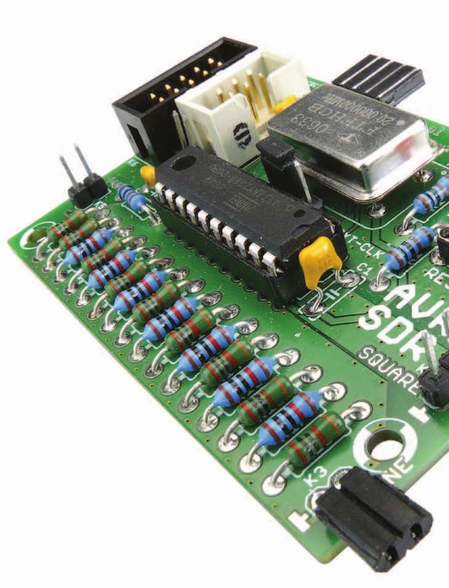
AVR SOFTWARE DEFINED RADIO

    AVR Software Defined
Generating precision signals using

By Martin Ossmann (Germany)

Atmel AVR
microcontrollers are very
popular, not least because of the free
development tools that are available. In this series we
shall show how these processors can be pressed into service for
digital signal processing tasks. We shall cover the subject from the ground
up, making the series suitable for beginners, and in true Elektor style the focus will be
on practical experiments. You can build the hardware yourself or you can obtain boards
from Elektor, and the software is as ever available for download as source code from our
website. Let’s generate some signals!

2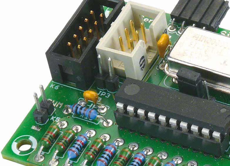
AVR SOFTWARE DEFINED RADIO
Radio Part 1
g an ATtiny micro
First a quick peek at what is in store in this series. The first board,
which includes an ATtiny2313, a 20 MHz oscillator and an R-2R DAC,
will be used to make a signal generator. The second board will fish
signals out of the ether. It contains all the hardware needed to make
a digital software-defined radio (SDR), with an RS-232 interface, an
LCD panel, and a 20 MHz VCXO (voltage-controlled crystal oscilla-
tor), which can be locked to a reference signal. The third board pro-
vides an active ferrite antenna. The software for all these projects
is written using the WinAVR GCC compiler in AVR Studio and can
be downloaded as C source code (plus fuse settings) or as hex files.
The series is built around practical experiments. We can look for-
ward to sine- and squarewave generators, an RMS voltmeter, experi-
ments in FM, AM and PM, FIR and IIR filters, wireless data trans-
mission, reception of the DCF timecode signal, RTTY weather mes-
sages, BBC long-wave radio transmissions and much more!
Before we get started, one word of warning: fluorescent energy-
saving light bulbs are based on switching regulators which splatter
interference all over the long-wave band. So we advise carrying out
the more sensitive experiments with the fluorescents off and the
mains halogen lights on (or by candlelight!).
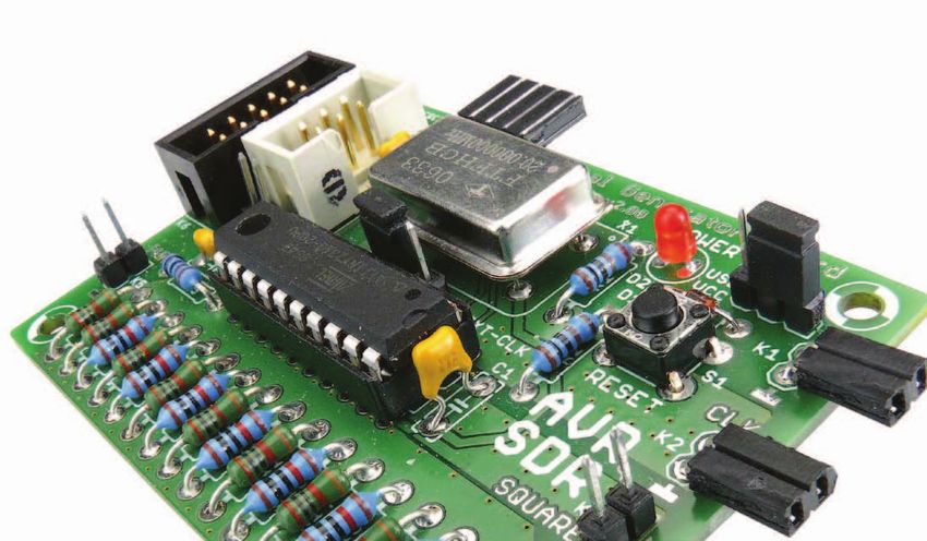
Signal generator board
The signal generator board is based on an AVR microcontroller
clocked at 20 MHz and an R-2R ladder forming a digital to analogue
converter to produce the output voltages. This is hardly a novel cir-
cuit, but we will show how it can be used in a wide range of applica-
tions. In particular we will use it to generate outputs useful for test-
ing other circuits, such as frequency- and phase-modulated signals.
Then, for even greater precision, we will connect the signal genera-
tor to an external clock source which is in turn locked to a frequency
Elektor Products and Support
• Signal generator kit including printed circuit board and all
components: # 100180-71
• BOB-FT232R USB-to-TTL converter, ready built and tested: #
110553-91
• USB AVR programmer, printed circuit board with SMDs fitted,
plus all other components: # 080083-71
• Free software download (hex files and source code): file #
100180-11.zip
All products and downloads are available via the web pages for
this article: www.elektor.com/100180
3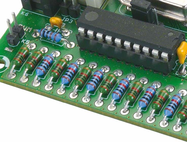
AVR SOFTWARE DEFINED RADIO
K7
VCC
2 1
4 3
6 5
VCC
ISP6
X1 The processor is clocked at 20 MHz by
K6
2 1
oscillator X1. It is a good idea to choose
JP3
a relatively high-precision component
EOH
4 3
JP2
6 5 here (50 ppm or better). Using a socket
CLK-SEL 8 7
20.000MHz makes it easier to try out different types
10 9
R18 of oscillator or oscillators of different fre-
20k
K2 ISP R17 quencies. Jumper JP2 allows the use of an
EXT-CLK
external clock signal, which should be
10k
VCC C1 R16 supplied at K2 (EXT-CLK).
20k
R15 The signal generator software programs
100n
20 allow a certain amount of external con-
RESET
MISO
MOSI
SCK
EXT
10k
VCC
5 R14 figuration using the microcontroller’s
+5VUSB PA0(XTAL1)
4 IC1 20k UART. The relevant pins are brought
PA1(XTAL2) R13
1
PA2(RESET)
ATTINY2313
out to a connector on the board (which
10k
+5V 19
PB7(SCL/PCINT7) is available from Elektor in the form of a
BOB-FT232R
TX 2 18 R12
PD0(RXD) PB6(DO/PCINT6)
RX 3 17 20k kit including all the components). The
PD1(TXD) PB5(DI/PCINT5) R11
GND 6
PD2(CKOUT/INT0) PB4(OC1B/PCINT4)
16 connector is suitable for directly attach-
10k
7 15
PD3(INT1) PB3(OC1A/PCINT3) ing the BOB-FT232R USB-to-serial
8 14 R10
9
PD4(T0) PB2(OC0A/PCINT2)
13 20k converter [1]. JP1 allows power to be
PD5(OC0B) PB1(AIN1/PCINT1) R9
11
PD6(ICP) PB0(AIN0/PCINT0)
12 obtained over the USB connection when
the unit is used with a PC: in this case no
10k
+5VUSB VCC GND
R8
10
20k
additional AC power adaptor is needed.
R7 Populating the printed circuit board (Fig-
JP1
ure 2) should present no particular diffi-
10k
D1
PWD-SEL
R6 culties: all the components are ordinary
20k
BAT85 D2
R2 R19 R5 leaded types. It is worth using a socket
for the processor in addition to the clock
1k
1k
10k
C2 R4 oscillator. Be sure to observe correct
20k
polarity on the programming connec-
K1 R1 100n K5 K4 R3 K3
S1 C3 tors K6 and K7. Programming can be
POWER
20k
1k
10n
done using the Elektor AVRprog [2]. It is
RESET PWM-LF SQUARE SINE
of course important to get the fuse con-
100180 - 11 figuration right: the source code gives
this along with the compiler options in
each case.
Figure 1. Circuit diagram of the signal generator. DDS sinewave generator
Our first application is a simple sinewave
generator programmed in C. The basic
sample clock is produced by one of the
standard such as the German DCF77 signal on 77.5 kHz or French timers built in to the microcontroller, arranged to trigger an inter-
TDF signal on 162 kHz. rupt. The interrupt routine is responsible for calculating the next
sample value of the sinewave (Figure 3). Call the kth sample S[k].
The circuit of the signal generator is shown in Figure 1. The central Writing p[k] for the phase of this sample, we have
component is the ATtiny2313 microcontroller, with the R-2R ladder
connected to port B forming the digital-to-analogue converter. The S[k] = sin (p[k]).
analogue output signal appears on K3 (SINE). Note, however, that
the output impedance of the circuit is relatively high at 10 kΩ. PWM Between one sample and the next the phase advances by a constant
output OC1A of the microcontroller is also available at K4 (SQUARE). value d (the ‘phase increment’):
We will use this output to generate square waves with frequencies
of up to a few hundred kilohertz, as well as to modulate other sig- p[k+1] = p[k] + d.
nals. Another PWM output, OC0B, is brought out to K5 (PWM-LF)
via a low pass filter comprising R19 and C3: this is suitable for gen- In a perfect sinewave generator these calculations must be carried
erating low-frequency analogue signals. out exactly, which of course is not practical. Instead, the direct digi-
4
AVR SOFTWARE DEFINED RADIO

  COMPONENT LIST
  Resistors                                        JP1,JP2 = 3-pin pinheader, lead pitch 0.1’’            K1,K2,K3 = 2-way receptacle, right-angled
  R1,R2,R19 = 1kΩ                                    (2.54mm) with jumper                                 BOB = 4-way receptacle, right-angled
  R5,R7,R9,R11,R13,R15,R17 = 10kΩ                                                                              K6 = 10-way ISP boxheader
  R3,R4,R6,R8,R10,R12,R14,R16,R18 =                                                                            K7 = 6-way ISP boxheader
   20kΩ                                                                                                        X1 = 20MHz quartz crystal (with 4
                                                                                                               receptacles Harwin type H3153F01)
  Capacitors                                                                                                   BOB-FT232R-001 = Elektor ‘BOB’ USB/
  C1,C2 = 100nF 100V                                                                                           TTL converter (ready assembled and
  C3 = 10nF                                                                                                    tested, # 110553-91)
                                                                                                               Printed circuit board
  Semiconductors
  D1 = BAT 85 (Schottky diode)                                                                                       Alternatively
  D2 = LED, green                                                                                                    Kit, including board and all parts: #
  IC1 = ATtiny2313-20PU, programmed                                                                                  100180-71.

  Miscellaneous
  S1 = pushbutton
  K4,K5 = 2-pin pinheader, lead pitch 0.1’’
    (2.54mm)
  JP3 = 2-pin pinheader, lead pitch 0.1’’     Figure 2. The printed circuit board is available from
    (2.54mm) with jumper                      Elektor as part of a kit including all the components.

tal synthesiser (DDS) stores the current phase value DDSp to finite          produce a fixed frequency output at 1 kHz; the result can be verified
precision as an m-bit number in the so-called ‘phase accumulator’.           on an oscilloscope (Figure 5). The interrupt service routine code is
One complete period of the sinewave corresponds to this value                shown in Listing 1.
covering the range of values from 0 to 2m–1. The same precision
is used for storage of the phase increment and for the phase addi-           Timing
tion operation.                                                              The DDS is clocked at fDDSCLK = 100 kHz. To generate a desired out-
                                                                             put frequency f the required phase increment is calculated using
The next step is to convert the phase value into the corresponding
sinewave sample. This is done using a look-up table which stores a                                        DDSd = 2n × f / fDDSCLK
complete sinewave period. If we were to store a sample for each of
the 2m possible values in the phase accumulator the table would be           and so for f = 1 kHz we have
unmanageably big: instead we use just the top n (where n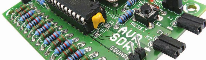
AVR SOFTWARE DEFINED RADIO

                Figure 5. Testing the sinewave generator.                             Figure 6. Measuring the execution time of
                                                                                            the interrupt service routine.

tine. As you can see from the code snippet above, we have brack-         As the output frequency f approaches fDDSCLK we start to observe
eted the calculation with commands to set and clear port pin PD.4.       undesirable artefacts such as jitter, noise and aliases in the output
This allows us to observe the execution time of the calculation using    spectrum. With a sample rate of 100 kHz it is best to keep f below
an oscilloscope: in this case we see a total time of around 2.2 µs.      about 10 kHz. Perhaps we can do a bit better if we use assembly
However, we must be careful as this does not include other con-          code?
tributions to the total time needed to service the interrupt: for
example, the time to save and restore processor registers will not       A faster DDS sinewave generator
be counted. However, with a relatively simple experiment we can          In order to make our sinewave generator capable of higher frequen-
determine these times as well.                                           cies we need to rewrite the DDS routine in assembler. With the help
Simply set up the main program as an infinite loop in which a port       of a cunning arrangement of variables in registers we can manage
pin (say PD.5) is toggled as quickly as possible. We can then observe    to get the sample rate of the 32-bit DDS as high as 2 MHz. The code
on the oscilloscope the periods when the toggling stops, which is        (Listing 2) uses the T flag to allow it to break out of its loop.
when the interrupt service routine is active: see Figure 6.              Our project now consists of a mixture of C and assembler code, and
In our experiment we measured the total time needed to process an        we need to store the sinewave table at a fixed address in memory.
interrupt at about 5.4 µs. The maximum allowable interrupt rate is       Configuring the project within WinAVR to achieve this is not a task
therefore 180 kHz. Adding a safety margin, we arrive at our figure       for the beginner. If you do not plan to make any changes to the code
of 100 kHz.                                                              it is probably best to program the ready-compiled hex file into the

    Listing 1
    ISR(TIMER1_OVF_vect) {
      PORTD |= _BV(4) ;                                            //   set sample timing flag
      PORTB=pgm_read_byte( SIN8+(DDSp>>24)) ;                      //   fetch and output sine sample
      DDSp += DDSd ;                                               //   advance DDS phase DDSp by DDSd
      PORTD &= ~ _BV(4) ;                                          //   clear sample timing flag
      }

    Listing 2
    loop:
        add      DDSphase0,DDSdelta0                 //     1     LSB of 32 bit DDS adder
        adc      DDSphase1,DDSdelta1                 //     1
        adc      DDSphase2,DDSdelta2                 //     1
        adc      ZL       ,DDSdelta3                 //     1     MSB is in ZL as pointer
        lpm      R0,Z                                //     3     access sine table
        out      PORTB,R0                            //     1     out to R-2R DAC on PORTB
        brtc     loop                                //     2 (1) loop until T flag set by interrupt routine
                                                     //     10 cycles in total for one loop

6
AVR SOFTWARE DEFINED RADIO

                                                                        frequency followed by CR and LF. The maximum usable signal fre-
                                                                        quency is about 200 kHz. The theoretical frequency resolution is
                                                                        given by

                                                                                     fDDSCLK / 2n = 2 MHz / 232 = 0.00046... Hz.

                                                                        To take advantage of this resolution the software allows you to
                                                                        enter a frequency with up to three digits after the decimal point,
                                                                        for example as ‘1000.045’ (followed by CR and LF). The internal
                                                                        calculations required to turn the entered frequency into a suitable
            Figure 7. Spectrum of the generated signal.                 parameter value for the DDS need to be carried out very accurately.
                                                                        To this end the author has written special-purpose arithmetic rou-
                                                                        tines, including one for fixed-point division.

processor (paying attention to the fuse bit settings). The project is   Figure 7 shows the spectrum of the sinewave output signal at fre-
called EXP-SinusGenerator-DDS-ASM-C-V01.                                quency f = 125.123 kHz over the range from 0 Hz to 2 MHz. As you
To make the sinewave generator more flexible it includes the abil-      can see, there are harmonics present, but all at more than 30 dB
ity to be configured over the UART interface (19200 baud, 8N1           below the desired signal. A low level of wideband noise is also vis-
data format). Using a terminal program, simply type in the desired      ible: this is a by-product of the DDS technique.

                                                                                                                                   Advertisement

    Fascinated by technology’s impact on
    the future?
    Check out Tech the Future!
    Computing power and global
    interconnectivity are pushing tech
    innovation into overdrive.
    Pioneering technologies and creative
    workarounds affect even the couch
    potato 24/7. Tech the Future reports
    on technology strides that shape
    the future — yours included.

    www.techthefuture.com
    Follow Tech the Future

                                                                                                                                              7
AVR SOFTWARE DEFINED RADIO

    Listing 3
    uint32_t DDS24 ;                                               // DDS phase, 24 bits used
    volatile uint32_t dDDS24 ;                                     // delta for DDS
    uint16_t TOP1 ;                                                // integer part of divider for PWM

    ISR(TIMER1_OVF_vect) {
      PORTD |= _BV(4) ;
      DDS24 += dDDS24 ;                                            // advance DDS phase
      if (DDS24 & 0x1000000UL ) {                                  // check bit 24 for overflow
         ICR1 =TOP1 ;                                              // on overflow PWM width = TOP1+1
         }
        else {
         ICR1 =TOP1-1 ;                                            // else PWM width = TOP1
         } ;
      DDS24 &=0xffffffUL ;                                         // make DDS24 24 bits again
      PORTD &= ~ _BV(4) ;
      }

If an ordinary crystal oscillator is used the overall accuracy of the     quencies. So for example if we alternate between using a divisor of
system will be in the region of plus or minus 100 ppm. In that con-       N and a divisor of N+1 then the overall effective division ratio will
text it hardly makes sense to claim that the generator can produce        be N+0.5. If a division ratio of 10.333... is wanted, then this can be
an output frequency of say 100.00005 kHz. For this reason the gen-        achieved by using a division ratio of 11 with ‘probability’ 0.333...
erator can accept an external 20 MHz clock signal, and in a later         and a division ratio of 10 the rest of the time.
instalment of this series we will see how such a clock can be derived     How can we use this in practice? We need an algorithm that will tell
from a transmitted reference. This combination allows the genera-         us, given the desired division ratio, when to divide by N and when
tion of sinewaves with excellent frequency accuracy.                      by N+1.
                                                                          Again, the m-bit DDS synthesiser comes to the rescue, with a suffi-
Trimming resonant circuits                                                ciently large value of m to achieve the desired precision. In this case
Later in this series we will use an AVR microcontroller to receive        we make use of the overflow of the phase accumulator. The rate p
and process longwave transmissions such as the DCF time code on           at which an m-bit phase accumulator overflows is just
77.5 kHz, France Inter on 162 kHz and BBC Radio 4 on 198 kHz. Usu-
                                                                                                      p = DDSd / 2m
ally a ferrite antenna will be used, and adjusting such an antenna can
be made much simpler using our sinewave generator: connect the
circuit up as shown in Figure 8 and adjust the trimmer capacitor for      and so we can control this rate as precisely as we need using the
maximum amplitude.                                                        variable DDSd. Whenever the accumulator overflows the timer is
                                                                          instructed to divide by N+1 rather than N on the next cycle.
It is possible to use the phase relationship between the output volt-     So, for example, if we wish to generate a 77.5 kHz squarewave from
age UOUT and the input voltage UIN to determine whether the reso-         a 20 MHz master clock, the required overall division ratio is
nant frequency of the circuit is higher or lower than that of the input
sinewave. If the phase of UOUT leads UIN then the sinewave frequency                         20000 / 77.5 = 258.0645161...
is lower than the resonant frequency; if UOUT lags UIN the signal fre-
quency is higher than the resonant frequency. When the frequen-           and so we need to divide by either N=258 or N=259 on each cycle.
cies agree UIN and UOUT are in phase.                                     The ‘probability’ of selecting N=259 will be p = 0.0645161..., which
                                                                          with a 24-bit DDS means that DDSd = p × 224 = 1082401. Listing 3
The example circuit shows component values for a resonant fre-            shows an interrupt service routine embodying this idea.
quency of 125 kHz; coil L1 is a small pot core inductor. We will use
this circuit later to generate test signals at a frequency of 125 kHz.    The squarewave produced by this code does of course suffer from
The trimmer capacitor can be adjusted to bring the resonant fre-          a small amount of short-term jitter, but in the long term the agree-
quency of the circuit to exactly 125 kHz: it is possible to use either    ment with the ideal frequency is excellent.
the signal from the R-2R ladder (K3) or the squarewave from the
PWM output (K4) to do this.                                               The whole routine, including interrupt overheads, has an execution
                                                                          time of about 6 µs, which means that we can use the technique to
PWM squarewave with a fractional divider                                  generate frequencies of up to about 160 kHz. Rewriting the routine
We will now look at another application of the DDS principle. If we       in assembler should allow considerably higher frequencies.
use a timer with a PWM output to generate a squarewave, we are            For convenience the squarewave generator program can also be
normally limited to producing frequencies that exactly divide the         controlled using a terminal. The source code is called EXP-Squar-
frequency at which the timer is clocked. If N is the division ratio       eGenerator-DDS-T1INT-V01.c in the downloadable zip archive [3].
and fCLK the timer’s clock frequency then the output frequency will       The fractional divider has many other applications. For example, it
be f = fCLK/N. However, if we adjust the division ratio on the fly (say   can be used to generate a signal with any desired sample rate, or
between N and N+1) then we can also produce intermediate fre-             form part of a digital PLL.

8
AVR SOFTWARE DEFINED RADIO

                                                                                          Uin           R1                         Uout
                                                                                                         100k

                                                                                                                L1
                                                                                                                            C2
                                                                                                                      C1
                                                                                                  R2
                                                                                                  10k                 1n5   500p
                                                                                                                1mH

FM generator
On its own the squarewave generator is perhaps not particularly
exciting. However, since controlling the PWM output does not
occupy all the processor’s time, we have some computing power
left over to change the frequency dynamically to make an FM                             Figure 8. Trimming a resonant circuit.
generator.
The German meteorological service [4] transmits weather informa-
tion on 147.3 kHz using frequency shift keying (FSK) in radiotele-
type (RTTY) format. Later in this series we will build a receiver capa-
ble of decoding these messages. To adjust and test the receiver it is
helpful to have a test signal. Using a fractional divider and the PWM
output this is easy: we just use a stream of data bits to control the
output frequency.
We will first program our test signal generator to work with a carrier
frequency of f = 125 kHz. A circuit along the lines of Figure 8 is used
to turn the squarewave output into a sinewave. We have already
seen the interrupt service routine for the fractional divider; the new
routine, ‘SendBit’, is responsible for sending a single bit (Listing 4).

First we wait for Timer 0 to run through COUNT2 cycles: in other
words, the bit rate is the Timer 0 overflow rate divided by COUNT2.
Then, depending on the value of the bit to be sent, the values of del-
taDDS24 and TOP1 are set. This is where the frequency modulation
occurs. Note that the commands that set these values are enclosed
between a cli() and sli() pair. If this is not done it is possible that
the interrupt service routine could be invoked when one parameter
has been changed but not the other, with potentially unpredictable
results. The routines can be found in the program EXP-SQTX-FM-                   Figure 9. Spectrum of a frequency-modulated signal
RTTY-V01.c. With further auxiliary routines we can transmit char-                                at 125 kHz ± 50 Hz.
acters using the Baudot [5] code, emulating the meteorological ser-
vice transmissions.

Figure 9 shows the spectrum of the FM RTTY signal. There are
two narrow peaks adjacent to one another, at frequencies of                Listing 4
125 kHz ± 50 Hz. The spectrum is continuous, falling off rapidly           void SendBit(uint8_t theBit) {
beyond ± 1 kHz.                                                              uint8_t k ;
                                                                             for (k=0 ; k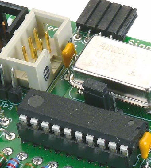
AVR SOFTWARE DEFINED RADIO

AVR Software Defined Radio (2)
Sampling signals
By Martin Ossmann (Germany)

As this series shows, the popular AVR microcontroller can
be used for digital signal processing tasks. Here we will
use an ATmega88 to sample amplitude- and phase-
modulated signals which we can either synthesise
ourselves or fish out of the ether. We can even
operate at frequencies of above 100 kHz.
How does it work? Read on to find out, in
theory and in practice.

A carrier wave can be used to send audio or data
through the ether by modulating it in amplitude, frequency
or phase. In a ‘software defined radio’ the first thing that happens
is that the received signal is sampled; then a processor carries out      with
the necessary calculations to recover the modulating signal. In the       a frequency of
case of data transmission, we then decode the signal into a stream        fRX = 2 kHz. We set the
of bits. To understand how this all works, we will first look at how      frequency fLO of the local oscil-
an analogue receiver operates.                                            lator (or ‘LO’) also to fLO = 2 kHz. In the
                                                                          upper branch of the circuit (which is called the
Reception, the analogue way                                               ‘in-phase’ or ‘I’ channel) the input signal is multiplicatively mixed
The input stage of many modern receivers looks like Figure 1 (where       with the cosine wave produced by the LO. This produces a DC com-
we have not shown the first stage of ‘preselection’ filtering). It        ponent X, which passes unchanged through the low-pass filter that
works as follows: suppose first that we want to receive a signal at Uin   follows. A component at 4 kHz is also produced, which is removed

                                                                                                            Y
                              I-channel
                                      U
                                           Low-pass          X                                   A sin( )

       U in                   cos
                                            Local
                                           oscillator                                                                          X
                        sin
                                                                                                                A cos( )

                                      V
                                           Low-pass

                              Q-channel

                   Figure 1. Quadrature mixing.                                          Figure 2. Geometrical interpretation.

10
AVR SOFTWARE DEFINED RADIO
by the low-pass filter. The value of X depends on the amplitude multiplies the samples of Uin by those of LOCOS. The result is the
A and phase ϕ of the input signal, the phase being measured sequence U = A, 0, A, 0, A, .... After the mixer this sequence is passed
relative to the output of the local oscillator. More precisely, through a low-pass filter. We can construct a simple low-pass filter
ignoring any gain in the low-pass filter, we have X = A cos ϕ. by calculating a rolling average of sequences of four consecutive
If the input signal is exactly in phase with the cosine output samples of U. For simplicity we multiply this result by 2, and the
of the local oscillator, X is maximised: this is why this branch is output of the filter is then X = A, A, A, A, A, ...; in other words, the
labelled ‘in-phase’. output is a constant with value A. X can be thought of as samples
Much the same happens in the lower branch of the diagram. The of a DC level of A, where A is exactly the amplitude of the original
difference is that the input is mixed with a sine signal (the cosine input signal.
signal with a 90 ° phase shift). The value of Y depends again on
the amplitude A and phase ϕ of the input signal, and we have Y = Now we turn to the quadrature branch. The inputs to this branch’s
A sin ϕ. Y is maximised when the input signal is 90 ° phase shifted mixer are the sequences Uin = A, 0, –A, 0, A, ... and LOSIN = 0, 1, 0,
with respect to the cosine output of the LO. For this reason, the –1, 0, .... The product of these sequences is V = 0, 0, 0, 0, 0, ...; in
lower branch is called the ‘quadrature’ channel. other words, the constant value zero. The result of low-pass filter-
Figure 2 shows the relationships graphically. The receiver can cal- ing V will also be zero.
culate the amplitude A and phase ϕ of the input signal from the The same argument can be applied when the input signal is a sine
values of X and Y. wave Uin = A sin (2π · 2 kHz · t), giving the results X = 0 and Y = A.
This shows that our discrete-time I-Q mixer works in just the same
Let’s get digital way as the classical analogue I-Q mixer described above. We have
Now let’s consider what happens when all the signals involved also seen that if the sample rate is four times the signal frequency,
are sampled at a sample rate fS = 8 kHz, exactly four times the fre- the output signals of the LO only take on the values zero, plus one
quency of the input signal (see Figure 3). and minus one. This in turn means that the digital mixer does not
The process of sampling converts the continuous-time input signal need a multiplier: we simply need to add and subtract the relevant
into a sequence of numbers. If the input signal Uin is a cosine wave input samples in the low-pass filter to calculate the values of X and Y.
with amplitude A and frequency 2 kHz (at the top of Figure 3), sam-
pling generates the sequence of values Uin = A, 0, –A, 0, A and so on. The hardware...
The values repeat every four samples, because we are sampling at A simple front end circuit (Figure 4) was designed to test this idea
four times the input frequency. on an AVR microcontroller. The analogue-to-digital converter inside
Let us look first at the in-phase channel and sample the cosine out- the ATmega88 is used to sample the input signal Uin and digitise it.
put signal of the local oscillator. The sequence of samples is LOCOS = The firmware then carries out the necessary calculations and the
1, 0, –1, 0, 1, .... Again, this repeats every four samples. The mixer results, X and Y, are output using PWM on pins OC0A and OC0B. To
+5V
K1
VCC
Y +5V
LED1
C2
A 100n
R5
A*cos(2 2kHz t) C1
K13
Uin 7 20
1k
ISP
t 10u
1 2 17
VCC AVCC
2
PB3 (MOSI) PD0 (RXD)
3 4 16 3
PB2 (SS) IC1 PD1 (TXD) R6 R7 K11
5 6 1 12
RESET PD6 (OC0A) 4k7 4k7
7 8 19 4
PB5 (SCK) PD2
9 10 18 5 C4 C3
1 15
PB4 (MISO) PD3 (OC2B)
6
DAC2
K5 C7 PB1 (OC1A) PD4
cos(2 2kHz t) t 23
PC0 (ADC0) PD7
13 10n 10n
R4 R1 24
470n PC1
+5V PC2
25 CLKout
470k
470k
ADC0
26
PC3 R8 R9 K10
21 11
AREF PD5 (OC0B) 4k7 4k7
1
X1 ATMEGA88-20
sin(2 2kHz t) t PB0
14 C6 C5
DAC1
9 27 R2
XTAL1 PC4
10 28 10n 10n
PB7 (XTAL2) PC5
1k
R3 20MHz GND AGND
C8 S1
8 22 LED2
470k
100n
RESET CLIPPING
100181 - 15
Figure 3. Sampling at four times the signal frequency. Figure 4. Hardware for a simple front end.
11AVR SOFTWARE DEFINED RADIO
+5V +12V +5V +5V'
LCD1 K1 IC1
JP3 3 D1 7805 D13 D14
1 1 3
4 x 20 R1
USB+5V
2
1N4007 1N5817 1N5817
2k7
K2
2
R21
LED+A
LED-C
C2
+5V
VDD
C1
VSS
R/W
+5V'
33R
RS
VL
D0
D1
D2
D3
D4
D5
D6
D7
E
0
D2 10u
1
2
3
4
5
6
7
8
9
10
11
12
13
14
15
R22 16 100u 25V 63V
10R
P3
C21 +5V'
10k 10u
63V L2
IC3 = 74HC04
1uH IC3F
13 12
+5V' 1
R6 R16 R15 C19 14
+5V'
2k2 IC3
IC3E
1k
1k
100n 7
T1
L1 11 10
D6 D7 1
R8
T2 4uH7
470k
BC560C D5 D8
R7
BF245B C7 C18
470k
K4 R5
ANT D12 D9
1 TP1 470R 100n 100n
2
D11 D10
21
20
P1
7
3 C5
+12V
AVCC
Mod1
AREF
VCC
C6
ANT1 R4
1k 100n
23
PC0 (ADC0)
100k 24
R2 470n PC1 (ADC1)
C4 25 2
PC2 (RXD) PD0 TX
10R
26 3
K3 PC3 (TXD) PD1 RX
100n R3 27 4
PC4 PD2 +5V
220R 28 IC2 5
C3 PC5 PD3 USB+5V BOB-FT232R-001
1 6
D3 R9 PC6 PD4
ANT2 10u 63V 1k (OC0B) PD5
11
CLKout
14 12
R10 CLIPPING PB0 (OC0A) PD6
15 13 R17 R19
470k PB1 PD7
K5 MOSI 16
PB2
1
4k7
4k7
K7 17 ATMEGA88
PB3
2 2 1 MISO 18 R20
+5V' PB4
3 4 3 SCK 19 4k7
PB5 K11
6 5 RESET 9 C16 C17
ADC0 10
PB6
ISP PB7 10n 10n
GND
GND
DAC1
IC3A IC3B IC3C K8
8
22
1 2 3 4 5 6
1 1 1 R18
K6
4k7
K12
R12 IC3D VCXO C14 C15
2M2
ADC1 R13 9 8
1 10n 10n
+5V' DAC2
2k2
C12
JP1 5p6 JP2
L3
B VCXO K10
A X1 1uH OSC
R11 C11
100k R14
+5V' 100p C9 IC4 IO2
470R
4
20MHz
C13 D4 C10 1 3
P2 100p E/D K9
C20 S1
470n 27p C8
20MHz
2
5.5-65p 100n
10k RESET IO4
SB1100 100181 - 11
Figure 5. Circuit diagram of our universal receiver board.
12AVR SOFTWARE DEFINED RADIO
COMPONENT LIST
Resistors (5%)
R1 = 2.7kΩ
R2,R22 = 10Ω
R3 = 220Ω
R4,R11 = 100kΩ
R5,R14 = 470Ω
R6,R13 = 2.2kΩ
R7,R8,R10 = 470kΩ
R9,R15,R16 = 1kΩ
R12 = 2.2MΩ
R17,R18,R19,R20 = 4.7kΩ
R21 = 33Ω
P1 = 1kΩ 20%, 0.15W trimpot
P2,P3 =10kΩ 20%, 0.15W trimpot
Capacitors
C1 = 100µF 25V, radial
C2,C3,C21 = 10µF 63V, radial
C4,C5,C7,C18,C19,C20 = 100nF 50V
C6,C13 = 470nF 63V
C8 = 5.5–65pF 150V trimmer
C9,C11 = 100pF 5% 100V
C10 = 27pF 2% 100V
C12 = 5.6pF ±0.25pF 100V
C14,C15,C16,C17 = 10nF 5% 50V
Inductors
L1 = 4.7µH, 190mA, 1.7 Ω
L2,L3 = 1µH, 270mA, 0.8 Ω
Semiconductors
D1 = 1N4007
D2,D3,D5–D12 = LED, red
D4 = SB1100
D13,D14 = 1N5817
T1 = BC560C
T2 = BF245B
IC1 = 7805
IC2 = ATmega88-20PU, programmed
IC3 = 74HC04
IC4 = 20MHz oscillator module Figure 6. The printed circuit board is available from Elektor
as part of a kit including all the components.
Miscellaneous
X1 = 20MHz quartz crystal, 50ppm
S1 = pushbutton SPST-NO, 6mm footprint
K4,K5,JP1,JP2 = 3-pin pinheader, lead pitch 0.1 4 IC pin receptacles (for IC4)
K1 = low voltage adapter socket
in. (2.54mm) Mod = 5-way pinheader for Elektor
K2,K6,K8 = 2-pin pinheader, right angled, lead
K7 = 6-pin pinheader, lead pitch 0.1 in. BOB-FT232R-001
pitch 0.1 in. (2.54mm)
(2.54mm) LCD1 = 4x20 LCD e.g. HC200401C-YF62L-VA
K3,K9–K12,JP3 = 2-pin pinheader, lead pitch
JP1,JP2,JP3 = jumper 0.1 in. (2.54mm) PCB # 100181-1
0.1 in. (2.54mm)
CLKout,TP1 = PCB solder pin
attenuate the PWM frequency component in these output signals, board (Figure 6) and all components. This is a good option, as popu-
each is passed though a two-stage RC low-pass filter. lating the board is not a tricky task. As you can see from the circuit
The circuit is straightforward enough to be built on a small piece of diagram the universal receiver board includes all the components
prototyping board. Things are made even easier if the Elektor uni- of the simple front end, but also allows for a wide range of addi-
versal receiver board is used: its circuit diagram is shown in Figure 5. tional future possibilities that we will look at later on in this series.
As was the case for the signal generator described in the first part of For example, it is possible to connect an active ferrite antenna: an
this series [1], this is available as a kit including the printed circuit example of such an antenna is again available as an Elektor kit, and
13AVR SOFTWARE DEFINED RADIO
Listing 1: Calculating the quadrature components
U=0 ;
if (sampleTime==0){ U= ADCv ; }
if (sampleTime==2){ U= - ADCv ; }
U3=U2 ; U2=U1 ; U1=U0 ; U0=U ;
X=U0+U1+U2+U3 ;
OCR0A=128+X/8 ; the signal generator and the program called EXP-SinusGener-
ator-DDS-ASM-C-V01; the wiper of the potentiometer is con-
V=0 ; nected to input ADC0 on the receiver board.
if (sampleTime==1){ V= ADCv ; } The analogue outputs DAC1 and DAC2 are connected to an oscillo-
if (sampleTime==3){ V= - ADCv ; } scope operating in X-Y mode. Then we instruct the signal generator
V3=V2 ; V2=V1 ; V1=V0 ; V0=V ; over its RS-232 interface to generate a 2 kHz sinewave [1] and adjust
Y=V0+V1+V2+V3 ; the amplitude of the signal using the potentiometer until the red
OCR0B=128+Y/8 ; LED (D3 in Figure 5) does not quite light. The front end is then being
driven to its maximum level, just short of clipping. The oscilloscope
should show a single point that moves slowly in a circle. In theory
the point should be stationary, but because the oscillator control-
the electronics and printed circuit board will be described in the ling the front end is not running at exactly the same frequency as
next instalment in this series. that controlling the signal generator, the point will move.
To see the effect more clearly, adjust the signal generator to pro-
... and the software... duce a frequency of 2005 Hz. Then the point will move in a circle
The software, as always, is available as source code and making five revolutions per second. With the signal generator set
as a hex file for download from the Elektor web site [2]. to 1995 Hz, the point will again move at five revolutions per sec-
For our first experiment the software we use is called ond, but in the opposite direction. Adjusting the amplitude of the
EXP-SimpleFrontend-2kHz-IQout-V01.c. input signal using the potentiometer affects the radius of the circle
The program samples the input signal at a rate of 20 MHz / 5000 = in which the point moves.
8 kHz. The signal is then mixed with a 2 kHz signal. A simple low- Our ‘I-Q demodulator’ has mixed the signal in the band around
pass filter then produces the X and Y outputs, which we can also 2 kHz down to a centre frequency of 0 Hz. Signals in sidebands
label as the quadrature components I and Q. above and below 2 kHz are now distinguished in the direction of
rotation of the point on the oscilloscope display. Now frequencies
Listing 1 shows the heart of this routine. The timer variable sam- around 2 kHz are of relatively little practical interest: more interest-
pleTime always counts cyclically from 0 to 3, and thus repre- ing are frequencies in the longwave bands used for sending data by
sents the current phase of the local oscillator. The variables U and various transmitters. This requires one further small step, as we shall
V are used to hold the values that are obtained by multiplying the see in the next section.
input value ADCv by the cosine sequence [1, 0, –1, 0] and the sine
sequence [0, 1, 0, –1] respectively. The values of U and V are then The road to RF
fed into a simple low-pass filter that calculates a rolling average over The Nyquist-Shannon sampling theorem states that a sample rate
sets of four samples. The results of this calculation, X and Y, are the of at least 2 f is required to represent losslessly a signal containing
in-phase and quadrature components of the signal and are written frequency components up to a frequency f. Using a lower sample
to the PWM registers OCR0A and OCR0B respectively. rate than this is called ‘undersampling’ or ‘sub-Nyquist sampling’.
Take a look at Figure 7. The time interval illustrated is 1 ms long.
... and, finally, testing The upper black curve is a cosine wave, with the corresponding
To test the receiver, we feed a sinewave signal from our signal gen- sine wave below, both at 10 kHz. As before, the signal is sampled at
erator into the front end hardware via a 10 kΩ potentiometer to 8 kSa/s (kilosamples per second), giving sample values indicated by
allow adjustable attenuation. We use the SINE OUT (K3) output of the small blue circles. With conventional sampling we need at least
two samples per period of the 10 kHz signal, but here we have less
than one sample per period: hence the signal is undersampled. The
sequence of sample values that we obtain is [1, 0, –1, 0, 1, 0, –1, 0,
1] for the upper signal and [0, 1, 0, –1, 0, 1, 0, –1, 0] for the lower
one. Superimposed on the figure, in red, are 2 kHz cosine- and sin-
ewaves. For these signals the sample rate of 8 kSa/s satisfies the
sampling theorem; but the surprise is that the 2 kHz signal and the
10 kHz signal give rise to the same set of sample values. This means
that a 10 kHz signal sampled at 8 kSa/s is indistinguishable from a
2 kHz signal sampled at the same rate. In turn this means that our
front end, which uses an 8 kSa/s sample clock, can equally well be
used to demodulate signals at 10 kHz.
Figure 7. Sampling a 10 kHz signal and a 2 kHz signal (red) There is of course a full theoretical analysis of the above phenom-
at 8 kSa/s. enon, known as the Nyquist-Shannon sampling theorem for band-
14AVR SOFTWARE DEFINED RADIO
BPSK and QPSK modulation schemes
A special case of phase modulation is binary phase shift keying
(BPSK), where the bit values zero and one are encoded by signals
180 degrees out of phase with respect to each other. This cannot
be done using the PWM method described in the text. However,
we can take advantage of the settings available in the AVR’s reg-
pass signals. One consequence of this theorem is that a sampled isters to select whether the event TimerValue == CompareValue
bandpass signal with bandwidth B starting at a multiple of the results in a positive-going or negative-going edge on the output:
sample rate fS can be reconstructed perfectly as long as B < fS / 2. in other words, we can selectively invert the PWM output. Intro-
In particular, we can reconstruct a bandpass signal with compo- ducing this possibility has the effect of adding a further circle to
nents stretching from n × fS to n × fS + fS / 2 for any chosen integer n; the diagram shown in Figure 11, as shown in the figure here.
or, stated another way, a bandpass signal centred at n × fS + fS / 4
with total bandwidth up to fS / 2. In particular, if we have a sample
rate of 8 kHz we can demodulate signals equally well around any
of the following frequencies: 2 kHz, 2 kHz + 1 × 8 kHz = 10 kHz, D = 0.5
2 kHz + 2 × 8 kHz = 18 kHz, 2 kHz + 3 × 8 kHz = 26 kHz, ..., 2 kHz +
20 × 8 kHz = 162 kHz, and so on. We can easily test this, for example A
by setting the signal generator frequency to 26005 Hz. D = 0.75 D = 0.25 B
B A
For undersampling like this to be successful the signal being sampled C
must be band-limited, for example by the insertion of a bandpass filter D
in front of the AVR. Image frequencies at n × fS – fS / 4 are also received: T
in our case these images are at 8 kHz – 2 kHz = 6 kHz, 2 × 8 kHz –
2 kHz = 14 kHz, ..., 25 × 8 kHz – 2 kHz = 198 kHz, and so on.
C D
So far we have assumed that the signal is perfectly digitised, and of
course that is not the case. The sample-and-hold stage in any ADC
has a so-called ‘aperture’, and a result of this is that it is not possible
to mix down very high frequencies using the AVR. However, in the
next part of this series, we will see how a signal transmitted by the In particular we now have four signal shapes (represented by
BBC on 648 kHz (in the mediumwave band!) can easily be decoded. the points A, B, C and D) that are spaced at 90 degree phase
intervals. This lets us implement QPSK (quadrature phase-shift
Amplitude and phase keying) modulation. If we restrict ourselves to just a pair of dia-
The signals X and Y give the strength of the in-phase and quadrature metrically opposite points (for example, A and C) we have the
components of the input signal. However, we are rather more inter- choice of two signals with phases 180 degrees apart: this gives us
ested in its amplitude A and phase ϕ, since one of our ultimate aims
BPSK modulation. Our PWM generator thus covers all the most
is to decode amplitude- and phase-modulated signals. If we had fast
important modulation schemes. They are all implemented in the
floating-point arithmetic we could compute the amplitude and phase
from the X and Y coordinates using the following two statements. program code and can be selected by invoking the appropriate
preprocessor directive.
A = sqrt(X * X + Y * Y);
PHI = atan2(Y, X);
The program EXP-SimpleFrontend-2kHz-Phase-Ampl-
V01.c calculates phase and amplitude using a rather more effi-
cient method and outputs the results on DAC1 and DAC2. The out-
put voltage level representing amplitude is logarithmically scaled,
enabling a direct conversion to dB. Figure 8 shows how the phase
of the signal transmitted by the BBC on 198 kHz changes over time.
The signal was received using an active ferrite antenna whose ampli-
fied output is fed into the receiver’s front end. Antenna input ANT2
on the receiver board can be used for this purpose, with pin 1 of
K4 linked to pin 2 of K5 so that the signal appears on input ADC0
of the microcontroller. Again we use a sample rate of 8 kHz. Since
198 kHz = 25 × 8 kHz – 2 kHz, the signal of interest is mixed down
to 2 kHz. The BBC transmission includes digital data sent using a
phase modulation of ±22.5 degrees at a rate of 25 bit/s. This digi-
tal modulation can clearly be observed in the mixed-down signal.
FM, PM and AM — with PWM
Next we want to try to generate some modulated signals ourselves. Figure 8. Phase modulation observed on a BBC 198 kHz
First install the program EXP-SQTX-125kHz-PWMa-V01.c into (Droitwich) transmission.
15AVR SOFTWARE DEFINED RADIO
Figure 9. Pulsewidth modulation: Figure 10. Pulsewidth modulation (D = 0.5 and D = 0.125).
amplitude shown in yellow, phase in blue.
the signal generator’s microcontroller. The 125 kHz squarewave varying by 0.4 V (which, as 1 V corresponds to 20 dB, means 8 dB).
output by this code is filtered using the resonant circuit described The phase variation is trickier to analyse. The first point to note is
in part 1 of this series [1] into a sinewave. Feed this signal into the that the phase jumps, in line with the data bit being transmitted,
ADC0 input of the receiver front end. This circuit arrangement will by about 0.92 V. This corresponds to 0.92 / 5 × 360 = 66 degrees.
be used for the following experiments. On top of this is superimposed a slow sawtooth signal with a slope
With the program E X P - S i m p l e F r o n t e n d - 1 2 5 k H z - (read from the oscilloscope trace) of about 5 V in 0.5 s. Now, 5 V cor-
Phase-Ampl-V01.c running in the front end the outputs will responds to a phase angle of 360 degrees, and so the phase angle is
represent the amplitude and phase of the received 125 kHz signal. making approximately two complete revolutions every second. The
Again the amplitude output is logarithmically scaled so that a wider reason for this is again that the transmitter and receiver have very
dynamic range can be represented: an output voltage of 4 V corre- slightly different ideas of what ‘125 kHz’ means: in fact, in this case
sponds to an input amplitude of 1 VPP and a step of 20 dB in ampli- they differ by 2 Hz. We will need to be careful to allow for this effect
tude gives a change of 1 V in the output level. A phase output volt- in future experiments. An error of 2 Hz in 125 kHz corresponds to
age of 5 V represents a phase angle of exactly 360 °. 16 ppm, which is rather better than the typical ±50 ppm tolerance
of a crystal oscillator. It is possible to compensate for this drift using
In the PWM code mentioned above a range of different modula- a PLL control loop to drive the oscillator in the receiver.
tion schemes and data sequences can be selected using #define pre-
processor directives. First we will try straightforward PWM, where A more refined kind of modulation
the frequency of a squarewave remains constant but its mark-space The above is all very well, but we would naturally like to implement
ratio is modulated. The bit transmission routine simply loads the pure amplitude modulation. And likewise, when implementing
modulating value into PWM register OCR1A (Listing 2). phase modulation, we would like to alter only the phase of the sig-
The period is fixed at 160, which means that the output frequency nal and not the amplitude. To that end we need to understand bet-
is 20 MHz / 160 = 125 kHz. The duty cycle is switched between D = ter what is happening in the PWM system.
80 / 160 = 0.5 and D = 20 / 160 = 0.125. Figure 9 is an oscilloscope Figure 10 shows the squarewave signal with the two different mark-
trace showing the resulting variation in amplitude and phase. It is space ratios D = 0.5 and D = 0.125, in each case accompanied by the
clear that both of these quantities are modulated, the amplitude sinewave signal that results after extracting just the fundamental
Listing 2: Modulation using simple PWM Listing 3: PWM modified for pure phase modulation
void bitSend(uint8_t theBit){ void bitSend(uint8_t theBit){
if (theBit) { if (theBit) {
OCR1A = 80 ; OCR1A = 80+10 ;
} }
else { else {
OCR1A = 20 ; OCR1A = 80-10 ;
} }
} }
16AVR SOFTWARE DEFINED RADIO
D = 0.5
D = 0.5 + R D = 0.5 – R
D* 180º
Figure 11. With judicious choice of mark-space ratios it is possible Figure 12. Pure phase modulation:
to achieve pure phase modulation. amplitude shown in yellow, phase in blue.
component using the 125 kHz resonant circuit. The filtered sine- origin of the plot inclined at an angle of D × 180 degrees to the
wave reaches its peak exactly in the middle of the squarewave pulse. point where it intersects the indicated circle. The length of this line
The mid-point moves when the mark-space ratio is changed, and so then gives the amplitude. As can be seen, the amplitude is maximal
there is a phase shift when the mark-space ratio is changed. when D = 0.5, and for any R, mark-space ratios of D = 0.5 – R, and
D = 0.5 + R give the same amplitudes. We can therefore use a pair of
In our example, when we use a mark-space ratio of D = 0.5 the phase such values to create pure phase modulation without an amplitude
angle is 0.5 × 180 degrees, or 90 degrees. When using a mark- component, and this is exactly what our PWM generator does when
space ratio D = 0.125 the corresponding phase angle is 0.125 × it is switched to PM mode using a #define directive. The essential
180 degrees, or 22.5 degrees. The difference between these two part of this code is shown in Listing 3.
phase angles is 90 – 22.5 = 67.5 degrees, which is in close agree- Figure 12 shows the result. The phase switches constantly between
ment with the measured value from Figure 9 of 66 degrees. the two values that represent zero and one. Superimposed on this
With a little more mathematics we can also calculate the amplitude is a small drift due to the frequency error. The amplitude (yellow
variation as a function of the mark-space ratio D. The peak-to-peak curve) is constant.
amplitude  of the sinewave is given by the formula
In the next instalment in this series we will look at how we can
 = 5 V × (4 / π) sin πD achieve pure amplitude modulation. However, we will not just be
looking at this in theory: we will also implement a DCF test trans-
and from this we can determine that the amplitude ratio between mitter and receive DCF signals. DCF is a German time standard
the cases D = 0.5 and D = 0.125 should be 0.3826834... = –8.343 dB. transmitter.
Again, this is in good agreement with the value of 8 dB measured (100181)
from Figure 9.
Internet Links
The relationship given above can also be illustrated graphically. Fig-
[1] www.elektor.com/100180
ure 11 shows how we can determine the amplitude that we will
obtain with a given mark-space ratio D. Construct a line from the [2] www.elektor.com/100181
Elektor Products and Support
• * Signal generator (kit including printed circuit board and all • * BOB-FT232R USB-to-TTL converter, ready built and tested: #
components): # 100180-71 110553-91
• * Universal receiver (kit including printed circuit board and all • * USB AVR programmer, printed circuit board with SMD parts
components): # 100181-71 fitted, plus all other components: # 080083-71
• * Active ferrite antenna (kit including printed circuit board and all • * Free software download (hex files and source code)
components): # 100182-71 All products and downloads are available via the web pages accom-
• * Combined kit (all three of the above): # 100182-72 panying this article: www.elektor.com/100181
17AVR SOFTWARE DEFINED RADIO
AVR Software Defined Radio
part 3
AM and FM, plus an active ferrite antenna
By Martin Ossmann (Germany)
As this series shows, the popular AVR microcontroller can be used for digital signal processing
tasks. In this instalment we will look at a few experiments involving amplitude and frequency
modulation, including a small DCF time code test transmitter. We will also extend the hardware by
adding an active ferrite antenna which will allow longwave and mediumwave signals to be received.
In the previous instalment of this series [2] tred on the point where the counter hits ister OCR1A is being switched between 8
we saw how a simple pulse-width modu- zero and thus has constant phase. If we filter and 40, which corresponds to switching the
lated (PWM) signal exhibits variations in the squarewave PWM output using a reso- mark-space ratio of the output between 0.1
both amplitude and phase. This means that nant circuit to generate a sinewave, we can and 0.5. The amplitude ratio in this case is
our basic signal generator cannot generate calculate the amplitude  of the result using sin (0.1 × π) / sin (0.5 × π) = 0.309016... =
a signal that is purely amplitude modulated. the formula  = A × (4 / π) sin (D × π), where –10.200 dB. Since the ‘amplitude’ output of
However, the PWM generator in the AVR D is the mark-space ratio of the squarewave the receiver has a scale of 1 V per 20 dB, the
microcontroller has some extra features and A its amplitude. voltage difference between the two levels is
allowing us to switch it to ‘phase correct’ This takes us neatly into our first experi- about 0.5 V (see the yellow trace).
PWM mode. In this mode the PWM coun- ment, which uses the signal generator and The other output of the receiver gives the
ter counts alternately upwards and down- the universal receiver board (or the ‘simple phase of the received signal. As can be seen
wards, between zero and a maximum value front-end’ described in [2]). The transmitter (blue trace) this is not affected by the mod-
specified in register ICR1. If this limit is 80, routine is simple in structure, as illustrated ulation. There is, however, a gentle drift
then a complete up-and-down cycle of the in the Listing. The software for the signal which is a result of the frequency difference
counter takes 160 clock cycles: if the clock generator, in file EXP-SQTX-125kHz- between the transmitter and the receiver.
runs at 20 MHz the basic PWM frequency PWMc-V01.c, is as usual available for
will be 125 kHz. Each time the counter value download from the project web pages [3]. DCF77, part one
passes the compare value set in register At the receiver end we use the program With what we have developed so far we can
OCR1A in either direction the correspond- EXP-SimpleFrontend-125kHz- build ourselves a DCF time code test trans-
ing PWM output bit is alternately set and Phase-Ampl-V01.c. mitter. The DCF77 time code transmitter is
cleared. Changing the compare value thus If we connect the two outputs of the located in Mainflingen, Germany, and has a
alters the mark-space ratio of the output receiver to an oscilloscope the result will range of about 1,200 miles. The carrier fre-
signal, but the output pulse is always cen- be as shown in Figure 1. The value in reg- quency of 77.5 kHz unfortunately does not
Uin L1 Uout
300 turns x 0.25 ECW
10 cm ferrite rod
C1 C2
330p 500p
Figure 1. AM modulation: amplitude in Figure 2. DCF77 transmitter tuned circuit. Figure 3. DCF77 reception. The short
yellow, phase in blue. and long pulses can be seen in the yellow
amplitude trace.
18AVR SOFTWARE DEFINED RADIO
second
of each Listing: Phase correct PWM
minute. void bitSend(uint8_t theBit){
T h e s of t- if (theBit)
ware {
includes a rou- OCR1A = 40;
tine that divides }
each one-second else
period into ten {
‘bits’ each lasting OCR1A = 8;
0.1 s. A short pulse is } // 10dB
sent using the bit pat- }
tern 0111111111, while
a long pulse uses the pat-
tern 0011111111. In the so that the input signal is taken to the ADC0
divide exactly into 20 MHz, and fifty-ninth second we send input of the ATmega. The software used is
so we have to use the fractional divisor 1111111111. The complete EXP-Simple-DCF77-RX-V01.c.
technique along with a 24-bit DDS accumu- message is built by concatenat- We sample the input signal at 10 kSa/s.
lator and a timer interrupt as described in ing these three templates. Since 77.5 kHz is exactly 8 × 10 kHz –
the first instalment of this series [1]. In this The program initialises the time to 11:41 10 kHz / 4, we can do the demodulation
new code, however, we will generate ‘phase on 15 August 2008. If the resonant circuit using the bandpass sub-Nyquist sampling
correct’ PWM, as we do not want any phase is correctly adjusted it is possible to set technique described in the previous instal-
modulation on the output. the time on DCF-controlled clocks within ment of this series. The oscilloscope traces
We feed the PWM output of the signal gen- a radius of a couple of metres. Most such in Figure 3 show the results. The upper
erator into a resonant circuit (Figure 2) con- devices correct their time only fairly infre- (yellow) trace shows the amplitude, with
sisting of a ferrite antenna and a suitable quently, but can usually be prodded into the short periods when the amplitude is
capacitor. An additional variable capacitor adjusting themselves by briefly removing reduced clearly visible. It is also possible to
allows us to trim the circuit for maximum the battery. see that both long and short reductions in
output amplitude. amplitude are present. Extracting the time
The code running in the ATtiny microcon- DCF77, part two information is now just a short step away.
troller in the signal generator is DCF_TX_ We would also like to be able to receive the We can also make use of the phase com-
V01.C, which produces messages com- real DCF time code from Germany. To do ponent of the DCF77 signal. In one of our
patible with the DCF77 time code. Each this we need the active ferrite antenna that later experiments we will clock the receiver
message is composed of pulses that start is described later in this article, and which is using a voltage-controlled 20 MHz crys-
at the beginning of each second, the time available as a kit from Elektor. The antenna tal oscillator (VCXO) rather than a fixed-
information being conveyed by whether the is connected to the ANT2 connection on frequency oscillator. If we adjust the fre-
pulse is a short or a long reduction in signal the receiver board. On the receiver board quency of the oscillator so that the phase
amplitude. No pulse is sent in the fifty-ninth itself we connect pin 1 of K4 to pin 2 of K5 no longer drifts, the 20 MHz signal will be
720°
360°
P(t)
0°
phase jumps
-360°
Figure 4. The same phase behaviour shown in two different ways. Figure 5. Frequency shift keying (FSK).
19AVR SOFTWARE DEFINED RADIO
+5V +12V +5V +5V'
LCD1 K1 IC1
JP3 3 D1 7805 D13 D14
1 1 3
4 x 20 R1
USB+5V
2
1N4007 1N5817 1N5817
2k7
K2
2
R21
LED+A
LED-C
C2
+5V
VDD
C1
VSS
R/W
+5V'
33R
RS
VL
D0
D1
D2
D3
D4
D5
D6
D7
E
0
D2 10u
1
2
3
4
5
6
7
8
9
10
11
12
13
14
15
16
R22 100u 25V 63V
10R
P3
C21 +5V'
10k 10u
63V L2
IC3 = 74HC04
1uH IC3F
13 12
+5V' 1
R6 R16 R15 C19 14
+5V'
2k2 IC3
IC3E
1k
1k
100n 7
T1
L1 11 10
D6 D7 1
R8
T2 4uH7
470k
BC560C D5 D8
R7
BF245B C7 C18
470k
K4 R5
ANT D12 D9
1 TP1 470R 100n 100n
2
D11 D10
21
20
P1
7
3 C5
+12V
AVCC
Mod1
AREF
VCC
C6
ANT1 R4
1k 100n
23
PC0 (ADC0)
100k 24
R2 470n PC1 (ADC1)
C4 25 2
PC2 (RXD) PD0 TX
10R
26 3
K3 PC3 (TXD) PD1 RX
100n R3 27 4
PC4 PD2 +5V
220R 28 IC2 5
C3 PC5 PD3 USB+5V BOB-FT232R-001
1 6
D3 R9 PC6 PD4
ANT2 10u 63V 1k (OC0B) PD5
11
CLKout
14 12
R10 CLIPPING PB0 (OC0A) PD6
15 13 R17 R19
470k PB1(OC1A) PD7
K5 MOSI 16
PB2
1
4k7
4k7
17
K7 PB3 ATMEGA88
2 2 1 MISO 18 R20
+5V' PB4
3 4 3 SCK 19 4k7
PB5 K11
6 5 RESET 9 C16 C17
ADC0 10
PB6
ISP PB7 10n 10n
GND
GND
DAC1
IC3A IC3B IC3C K8
8
22
1 2 3 4 5 6
1 1 1 R18
K6
4k7
K12
R12 IC3D VCXO C14 C15
2M2
ADC1 R13 9 8
1 10n 10n
+5V' DAC2
2k2
C12
JP1 5p6 JP2
L3
B VCXO K10
A X1 1uH OSC
R11 C11
100k R14
+5V' 100p C9 IC4 IO2
470R
4
20MHz
C13 D4 C10 1 3
P2 100p E/D K9
C20 S1
470n 27p C8
20MHz
2
5.5-65p 100n
10k RESET IO4
SB1100 100182 - 13
Figure 6. Circuit diagram of the AVR-SDR universal receiver board.
locked to the very precise carrier frequency 360 degrees = 5 V and 0 degrees = 0 V. The
of the DCF77 transmitter. In Figure 3 it is wrap-around appears sudden on the oscil-
L1
possible to see the phase changing slowly: 4mH7
loscope trace, but the underlying physical
R10 C1 R1
by using a phase-locked loop it is possible behaviour is continuous.
470R
470R
T1 47u
to automate the adjustment, as we shall 25V We can often get a clearer picture if, rather
see later in this course. It is also possible to K1 T2 BC560C T3 than restricting the angle to lie between
L2 Antenna
lock the receiver to other sources, such as C4 0 degrees and 360 degrees, we allow it to
BBC Droitwich transmissions on 198 kHz or BF245B TP1 BC550C
K2
go below 0 or beyond 360. In Figure 4 on
C3 R2 C2
France Inter on 162 kHz, both of which also R9 R8 R7 R6 R5
470R the left we can see a representation in this
100n 100n
provide very precise frequency references. R4 R3 form of a phase-modulated signal with a
220R
100R
47R
22R
10R
470R
frequency offset superimposed. The curve
4k7
10
2
4
6
8
Understanding JP1 is rather easier to interpret than when the
the phase changes phase angle is restricted.
1
3
5
7
9
100182 - 14
Figure 1 shows the by now familiar saw- A couple of analogies may help to explain
tooth pattern in the phase angle that results what is happening. First imagine walk-
from a frequency offset between trans- ing in a circle around the north pole: at a
mitter and receiver. The phase changes Figure 7. Circuit diagram of the active certain point, which has no particular sig-
smoothly, wrapping round bet ween ferrite antenna. nificance on the ground, your longitude
20AVR SOFTWARE DEFINED RADIO
will jump between 180 degrees west and
180 degrees east. Now imagine not walk-
ing in a circle, but climbing a spiral staircase.
After one complete revolution you are not
in exactly the same place: you are one floor
higher. If, along with the phase angle, we
keep track of which ‘floor’ we are on, we
can represent phase differences of more
than 360 degrees. This is a technique used
in constructing PLLs that have a wide cap-
ture range. Figure 8. The author’s prototype of the active ferrite antenna.
Figure 5 shows a nice application of this
technique. We use our signal generator as
an FSK (frequency shift keying) transmit- couple of extra filters can be added to make Analogue signals are presented to the
ter, using the software in EXP-SQTX-FM- the receiver more robust. microcontroller on the ADC0 input to its
RTTY-V01.c. The output of the signal gen- analogue-to-digital converter. R7 and R8
erator on K4 is taken via a resonant circuit The universal receiver board provide a DC offset voltage on this input
acting as a filter (see the first part of this Now that we have carried out a few experi- equal to half the converter’s reference
series [1]) to input ADC0 on the receiver. ments with the simple receiver circuit, it voltage AREF, while C6 provides AC cou-
The code running in the receiver is EXP- is time to move on to a more advanced pling for the input. T1 and T2 form a pre-
SimpleFrontend-125kHz-extPhase- receiver board. The universal receiver board amplifier to whose input (K4 pins 2 and 3)
Freq-V01.c, which has a phase output was described, including a printed circuit a resonant receiver circuit consisting of a
scaled so that it can represent a wider range board layout, in the previous instalment of ferrite antenna and a tuning capacitor can
of phases. The scaling is such that 5 V rep- this series. Figure 6 shows the circuit dia- be directly connected. The output of the
resents 8 × 360 degrees. The 125 kHz car- gram again to help explain some of the preamplifier can be fed to the ADC input
rier generated by the transmitter is shifted interesting possibilities that it opens up. A by connecting together pins 1 and 2 of K5.
by +/– 50 Hz to represent the bits 1 and 0, four-line LCD panel is provided as a display. Another possibility is to connect a ferrite
and the data rate is 50 bits per second. A Header Mod1 allows a BOB-FT232R USB- antenna with phantom power to the pre-
shift of +/– 50 Hz means that in one bit to-TTL converter to be added: this lets you amplifier input: in this case pins 1 and 2 of
time, 1/50 s, the transmitted signal will communicate between the board and a PC, K4 should be connected together and the
gain or lose one period relative to the refer- for example to log received data. ferrite antenna connected to K3.
ence signal. Each bit thus corresponds to a A discrete 20 MHz oscillator is provided as a For some of the experiments we have seen
phase shift of 360 degrees with a direction clock source. The frequency of this oscillator so far (and for some in the future) we have
that depends on the value of the bit being can be adjusted over a narrow range using generated two outputs from the receiver
sent. In turn, a phase change of 360 degrees a control voltage. This voltage is derived and visualised them using an oscilloscope.
gives a change in the output voltage of 5 V / either from potentiometer P2 or from the These outputs are generated using PWM
8 = 0.625 V, and this occurs over a period of AVR microcontroller itself via PWM output based on Timer 0 and are available on pins
20 ms. The blue trace in Figure 5 shows this OC1A/PB1 and a lowpass filter comprising OC0A and OC0B. Each of these is equipped
effect clearly. R10 and C13. This latter option allows the with a two-stage RC filter. The resulting
Demodulating the FSK signal is easy: the VCXO to form part of a phase-locked con- voltages are available on K11 and K12.
instantaneous rate of change of phase cor- trol loop, for example to derive a precision
responds to the current frequency shift and frequency reference from the DCF77 signal. Active ferrite antenna
hence to the transmitted bit. The rate of A divided-down version of the clock fre- To complete the picture we equip our
change of phase can be calculated by taking quency can be output on pin OC0B. Alter- receiver with an active ferrite antenna for
the difference between consecutive phase natively, an integrated quartz crystal oscilla- the longwave and mediumwave bands.
values: the result is shown in the yellow tor module (IC4) can be selected to provide Figure 7 shows the circuit diagram. Thanks
trace. When the phase angle is increasing the master clock using jumper JP2. to JFET T2 the input has a very high imped-
the yellow trace is ‘high’; when it is decreas- Ports C and D are used to drive eight LEDs ance, and so the tuned circuit forming the
ing, the trace is ‘low’: from this is it easy arranged in a circle that can be used as antenna has a high Q-factor and selectivity.
to read off the bits being sent. A software a phase display. These provide a simple T1 provides a useful amount of gain and
UART can be added to make a complete means of determining when the PLL is in emitter follower T3 gives a low-impedance
software defined FSK receiver. In the next lock, and give a clear indication when a output. Resistor R2 gives negative feedback
instalment of this series we will see how a small frequency offset is present. for DC and AC, the latter being configurable
21You can also read