Enhanced flexible optoelectronic devices by controlling the wettability of an organic bifacial interlayer - Nature
←
→
Page content transcription
If your browser does not render page correctly, please read the page content below
ARTICLE
                  https://doi.org/10.1038/s43246-021-00131-4                OPEN

                  Enhanced flexible optoelectronic devices by
                  controlling the wettability of an organic bifacial
                  interlayer
                  Soyeon Kim1,5, Adi Prasetio 1,2,5, Joo Won Han2, Yongki Kim3, Myunghun Shin3, Jinhee Heo1, Jung Ha Kim2,
                  Shinuk Cho 4, Yong Hyun Kim 2, Muhammad Jahandar 1 ✉ & Dong Chan Lim 1 ✉

                  Solution-processed flexible organic optoelectronic devices have great potential as low-cost
                  organic photovoltaics for energy harvesting, and in organic light-emitting diodes as a lighting
1234567890():,;

                  source. However, a major challenge for improving device performance and stability is the
                  different interfacial characteristics of the hydrophobic organic layers and hydrophilic trans-
                  parent electrodes, particularly for flexible devices. Surface wetting controlled interfacial
                  engineering can provide a useful method to develop highly efficient flexible organic devices.
                  Here, an unsaturated fatty acid-modified ethoxylated polyethyleneimine organic interfacial
                  layer is designed, which is hydrophobic or hydrophilic on different interfaces. This interlayer
                  results in a power conversion efficiency of 10.57% for rigid and 9.04% for flexible photo-
                  voltaic devices. Furthermore, the long-term air storage stability for 250 h is substantially
                  improved, retaining 87.75% efficiency without encapsulation, due to the wettability driven
                  improvement of the optical and electronic properties of the cathode interfacial layer. The
                  performance of organic light emitting diodes also benefitted from the interlayer. This study
                  provides a strategy to simultaneously improve efficiency and stability by controlling the
                  wettability of the interfacial layer.

                  1 Surface Technology Division, Korea Institute of Materials Science (KIMS), Changwon, Republic of Korea. 2 Department of Display Engineering, Pukyong

                  National University, Busan, Republic of Korea. 3 School of Electronics and Information Engineering, Korea Aerospace University, Goyang, Republic of Korea.
                  4 Department of Physics and Energy Harvest Storage Research Center (EHSRC), University of Ulsan, Ulsan, Republic of Korea. 5These authors contributed

                  equally: Soyeon Kim, Adi Prasetio. ✉email: jahandar@kims.re.kr; dclim@kims.re.kr

                  COMMUNICATIONS MATERIALS | (2021)2:26 | https://doi.org/10.1038/s43246-021-00131-4 | www.nature.com/commsmat                                            1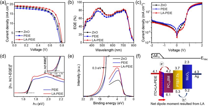
ARTICLE                                                            COMMUNICATIONS MATERIALS | https://doi.org/10.1038/s43246-021-00131-4

O
         ver the past few decades, organic semiconductor optoe-            Moreover, Zhang et al. also reported two nonconjugated poly-
         lectronic devices, such as organic photovoltaics (OPVs)           mers PEIE-DBO and PEIE-DCO developed by quaternization of
         and organic light-emitting diodes (OLEDs) have gar-               PEIE with 1,8 dibromooctane (DBO) or 1,8 dichlorooctane
nered considerable attention owing to their remarkable intrinsic           (DCO) to improve electron mobility and conductivity32. The
properties. These properties include solution processability, good         PEIE doped by tetraalkylammonium salts also was developed to
mechanical flexibility, and easy and low-cost manufacturing                 further reduce the WF by a combination of the alignment of the
(printing or roll-to-roll fabrication) techniques1–7. Moreover,            permanent dipole of PEIE and ionic electric polarization along
with excellent color tunability and free-form design, OPVs and             the depth direction on electrodes33. However, from the reported
OLEDs show prominent and wide-ranging advantages for com-                  studies, the wetting properties at the electrode/active layer
mercial applications5,8,9. Recently, OPVs have been reported to            interface is not yet intensely investigated.
exhibit a power conversion efficiency (PCE) of over 18% (non-                  In this study, we demonstrated highly efficient flexible OPV
fullerene acceptor), which set a new landmark for high-                    and OLED devices using modified PEIE CILs with different
performance OPVs to overcome the energy crisis10. On the                   hydrophilicity on both sides of the layer. The different hydro-
other hand, OLEDs have achieved vivid RGB (red–green–blue)                 philicity of the CILs can adjust the heterogeneous bifacial inter-
color and high-brightness white light. These OLEDs have already            layer properties between the organic active layer and transparent
been commercialized in the display and lighting market7.                   conducting ITO electrode. A novel Janus PEIE CIL was prepared
   For developing integrated photovoltaics and large-sized, yet            by adding hydrophobic organic molecules, such as fatty acids in
lightweight, flexible displays, the flexibility of OPVs and OLEDs is         the PEIE. Fatty acids consist of a polar head, –COOH, and chains
highly desirable. Generally, polyethylene naphthalate (PEN) and            of an uncharged, nonpolar tail, which are hydrophobic in nature.
polyethylene terephthalate (PET) are used as substrates for fab-           The polar head of the fatty acid simply reacted with the hydroxyl
ricating flexible optoelectronic devices. However, these substrates         group of PEIE and/or created bonds with the ITO surface by
become unstable when thermally annealed over 120 °C for PEN                acting as an anchoring group. The long hydrophobic chain of the
and 78 °C for PET7,11,12. Thus, the room temperature fabrication           fatty acid partially exposed the top surface of the PEIE CIL and
process is strongly preferable for developing flexible optoelec-            transformed it into a hydrophobic surface. In addition, the opto-
tronic devices. However, flexible devices, particularly those with          electrical characteristics, such as electrical conductivity, band gap,
inverted structures, still underperform as compared to the rigid           and dipole moment were also improved.
devices. The electron transport or material properties of the                 In general, two groups of fatty acids exist: saturated fatty acids
electron injection layer are important for extracting or injecting         (SFA) and unsaturated fatty acids (UFA). In this study, PEIE was
electrons while blocking hole transport, which is more effective           modified using saturated stearic acid and unsaturated linoleic acid
when using rigid substrates or high-temperature manufacturing              with an equal number of carbon atoms, which are denoted as SA-
processes.                                                                 PEIE and LA-PEIE, respectively. The LA-PEIE based flexible
   Metal oxides, such as zinc oxide (ZnO), tin oxide (SnO2), and           OPV and OLED devices have excellent properties, which are
titanium oxide (TiO2), have a wide bandgap, high electron                  superior to those of the pristine PEIE, and ZnO CILs. These
mobility, and environment-friendly characteristics. As a result,           properties particularly include: (i) the interfacial charge transport,
they are commonly used to fabricate highly efficient optoelec-              (ii) device stability under ambient conditions, and (iii) mechan-
tronic devices13–20. However, ZnO, SnO2, and TiO2 interfacial              ical durability of the device during bending tests. The OPV
layers are commonly fabricated using a high-temperature                    devices that used LA-PEIE as the CILs and PTB7‐Th: PC70BM
annealing process, which is not suitable for developing flexible            bulk‐heterojunction as the active layers achieved a remarkably
optoelectronic devices. Thus, to improve the performance of the            high PCE of 10.57% (flexible OPVs achieved 9.04% of PCE),
OPVs and OLEDs, many researchers have employed organic                     whereas the devices that used the pristine PEIE CIL achieved a
cathode interfacial layers (CILs) of different materials, such as          PCE of 9.30% (flexible OPVs achieved 7.87% PCE). To the best of
Poly [(9,9-bis(3’-(N, N-dimethylamino)propyl)-2,7-fluorene)-alt-            our knowledge, these results indicate the highest achieved PCEs
2,7-(9,9–dioctylfluorene)] (PFN) and its derivate (PFN-V                    for the widely studied PTB7‐Th: PC70BM devices with
and PFN-Br) or polyfluorene derivative (WPF-Oxy-F) and Poly                 polyelectrolyte CILs.
[(9, 9-bis (6′-diethoxylphosphorylhexyl) fluorene)] (PF-EP)21–25.
Among these materials, polyethylenimine 80% ethoxylated
(PEIE), a low-cost commercial polyelectrolyte, has been exten-             Results
sively used for fabricating flexible optoelectronic devices. This is        Optoelectronic properties and morphology of CILs. To study
because PEIE can perform well even without thermal annealing               the optoelectronic properties and morphology of the CILs, we
treatment owing to its excellent mechanical flexibility14,26–29. The        compare the transmittance spectra of bare glass, ITO glass, and
aliphatic amine groups that are present in the PEIE can align the          ITO PEN substrates (see Supplementary Fig. S2a). The high
permanent dipole at the indium tin oxide (ITO)/photoactive layer           absorption of the ITO PEN in the ultraviolet (UV) region is due
interface. This alignment lowers the electron injection barrier to         to the naphthalene rings in the PEN main chain30. The trans-
reduce the trap-assisted recombination26,28,29. Nevertheless, the          mittance spectra of the ZnO, PEIE, and LA-PEIE films that are
nonconjugated PEIE, which is an electrical insulator, weakens the          deposited on ITO glass substrates are shown in Supplementary
charge extraction or injection of the substrate material. In addi-         Fig. S2b. Both PEIE and LA-PEIE films exhibit similar light
tion, the hydrophilic tail of PEIE deteriorates the long-term              transmittance characteristics. Surface roughness and organic
device stability28,30 and prevents the uniform deposition of the           hydrophobicity are the prerequisites for fabricating super-
organic active layer on the PEIE treated ITO substrate31. Thus,            hydrophobic surfaces. Low surface energy and texture with nano-
the structural engineering or modification of the PEIE molecule is          or micro-texturing alter the surface characteristics and turn the
crucial to improve its capability as the interfacial layer for the         surface hydrophobic. The surface morphologies of the CILs were
development of flexible optoelectronic devices. To improve the              observed via atomic force microscopy (AFM). The corresponding
performance of OPV devices based on PEIE CILs, many studies                AFM images are shown in Fig. 1b, c. The surface (0.48 nm, which
have been attempted. For example, Zhang et al. modified the                 is a root mean square (rms) value) of the LA-PEIE film is
PEIE by a simple quaternization reaction between PEIE and 1,8-             smoother than that of the PEIE film (0.75 nm rms). A smoother
diiodooctane (DIO) to improve the thickness dependency30.                  surface helps in a seamless transition from the CILs to active

2                      COMMUNICATIONS MATERIALS | (2021)2:26 | https://doi.org/10.1038/s43246-021-00131-4 | www.nature.com/commsmat
COMMUNICATIONS MATERIALS | https://doi.org/10.1038/s43246-021-00131-4                                                               ARTICLE

Fig. 1 Mechanism and behavior of fatty acid modified PEIE CILs. a Schematic of the mechanism of PEIE and LA-PEIE CILs. b, c AFM images of PEIE and
LA-PEIE CILs with rms of 0.75 and 0.48 nm, respectively. d, e Contact angle images of PEIE (θ = 25.85o) and LA-PEIE (θ = 58.62o). f Fourier transform
infrared spectroscopy (FTIR) spectra of PEIE (blue line) and LA-PEIE CILs (red line).

layers without defects, allowing for better charge extraction34–36.            hydrophobic molecules (fatty acids) into PEIE can create a bifa-
Several reports mentioned that CILs with textured rough surfaces               cial interface that is hydrophilic at the bottom surface facing the
(nanowires, nanowall, and ripples) are a more suitable archi-                  ITO layer and hydrophobic at the top surface facing the photo-
tecture for enhancing the electrical and mechanical properties of              active layer. The bifacial property of the LA-PEIE CIL also
the interface between the CILs and the active layer37–39. A                    increases the contact angle and strength of the induced surface
stronger hydrophobicity is expected on the rough surface of the                dipoles. Thus, compared to the PEIE CILs, the photoactive layer
PEIE film (Fig. 1b, c). However, a higher hydrophobicity is                     can be coated more uniformly on the LA-PEIE CILs, thereby
observed on the smooth LA-PEIE film surface (Fig. 1d, e), which                 improving the adhesion of the LA-PEIE with the photoactive
was previously treated by a linoleic fatty acid. The addition of LA            layer when spin-coated using a hydrophobic chlorobenzene sol-
increased the contact angle; the contact angle of LA-PEIE (58.62°)             vent31, as illustrated in Fig. 1a. The excessive phase separation
is higher than that of the PEIE (25.85°). The improved hydro-                  and aggregated PC70BM occurred when the photoactive layer was
phobicity of the LA-PEIE film is a consequence of the formation                 coated on the PEIE with a hydrophilic surface, resulting in poor
of the hydrophobic tail of LA on the top surface of the PEIE                   device performance (Supplementary Fig. S3a). Meanwhile, the
layers. This improvement in the hydrophobicity is confirmed by                  photoactive layer coated on the hydrophobic surface of LA-PEIE
performing Fourier transform infrared spectroscopy (FTIR) of                   has lower roughness (Supplementary Fig. S3b), indicating a better
the films (Fig. 1f). For both PEIE and LA-PEIE samples, the                     morphology of D/A photoactive materials. Therefore, the bifacial
absorption peaks at 1047 and 1460 cm−1 can be attributed to                    LA-PEIE CILs can improve the performance of flexible optoe-
C–N and C–O bonds, respectively. The carboxylic group (C=O)                    lectronic devices.
and C=C are observed respectively at 1659 and 1565 cm−1,
which indicates that LA is well incorporated with PEIE. The
absorption of O–H is observed in the range of 3200–3500 cm−1.                  Device performance of ITO/glass-based OPVs. To determine
In this range, the decrease in absorption by the O–H bond in LA-               the dependency of device efficiency on the hydrophobic char-
PEIE indicates a decrease in the number of OH hydrophilic sites.               acteristics of the PEIE CILs, we fabricated devices with different
These results are further confirmed by the Raman spectra (Sup-                  LA concentrations. The variation of the performance of a rigid
plementary Fig. S10). The C=O and C=C bonds indicating                         OPV device with the contact angle owing to the LA concentration
the incorporation of LA with PEIE are observed at 1697 and                     and its effect are shown in Supplementary Fig. S3c and tabulated
1648 cm−140–43 Furthermore, the intensity of peak corresponding                in Supplementary Table S1. As expected, the device performance
to O–H bending is observed decreased. It implies that the con-                 is strongly affected by the hydrophobicity based interfacial
centration of the hydroxyl group in PEIE is decreased after the                characteristics. As we increased the LA concentration, the PCE of
incorporation of LA42,44,45. The hydrophilic sites of PEIE can                 the OPVs increased to a certain value with enhanced hydro-
easily react with the OH groups in the fatty acids. This suggests              phobicity and then decreased (see Supplementary Fig. S3d). The
that most of the fatty acid hydrophobic chains are located on one              decreased PCE can be interpreted as the nonconducting effect of
side of the LA-PEIE film, depending on the surface condition of                 the excessive amount of the LA hydrophobic chain. The current
the substrate, while the hydrophilic hydroxyl chains are located               density–voltage (J–V) curve and external quantum efficiency
on the other side. In this manner, the incorporation of organic                (EQE) of the best OPV on a rigid substrate are shown for each

COMMUNICATIONS MATERIALS | (2021)2:26 | https://doi.org/10.1038/s43246-021-00131-4 | www.nature.com/commsmat                                       3
ARTICLE                                                                                     COMMUNICATIONS MATERIALS | https://doi.org/10.1038/s43246-021-00131-4

Fig. 2 Photovoltaics performance and energy level alignment. a Current density–voltage characteristics, b EQE spectra, and c dark J–V of various CILs.
d [hv ln(1−EQE)]2 vs hv curve of PEIE (blue line) and LA-PEIE (red line) with Tauc plot. The straight-black line represents the extrapolation. e UPS spectra
of ZnO (black line), PEIE (blue line) and LA-PEIE (red line) on ITO substrates. f Energy level diagram of an OPV device with the structure of ITO/LA-PEIE/
PTB7-th:PC70BM/MoOx/Ag.

 Table 1 The detailed device performance parameters of the rigid and flexible OPV devices based on PTB7-th:PC70BM
 photoactive layer with various CILs.

 CILs                          Type of OPV cells                          PCE (%)                      FF (%)                 VOC (V)                JSC (mA cm−2)
 ZnO                           Rigid                                       9.46   (9.30)               0.67 (0.66)            0.80 (0.79)            18.63 (18.12)a
                               Flexible                                    6.41   (6.04)               0.53 (0.52)            0.79 (0.76)            15.28 (15.19)
 PEIE                          Rigid                                       9.30   (8.95)               0.66 (0.65)            0.80 (0.79)            17.73 (17.43)
                               Flexible                                    7.87   (7.59)               0.64 (0.64)            0.76 (0.76)            15.53 (15.46)
 LA-PEIE                       Rigid                                      10.57   (10.25)              0.68 (0.66)            0.82 (0.81)            19.33 (19.11)
                               Flexible                                    9.04   (8.80)               0.66 (0.65)            0.80 (0.79)            16.99 (16.78)
 aThe   values in parentheses stand for the average performances from over 12 cells.

CIL in Fig. 2a, b. In addition, the photovoltaic properties of each                               the conjugated chains in LA lead to form higher dipole moment
device are summarized in Table 1. The ZnO CILs exhibited a                                        compared to SA. The calculated dipole moments for LA and SA
higher PCE (9.46%) as compared to the PEIE CIL, mainly because                                    are 1.61 and 1.48 D, respectively. Thus, the reinforced dipole
of the higher fill factor (FF) of the ZnO CILs. The OPV with LA-                                   moment of LA-PEIE is higher than those of SA-PEIE as illu-
PEIE CIL outperformed the OPVs with other CILs and showed                                         strated in Supplementary Fig. S4b.To gain deeper insights into the
the highest PCE (10.57%), FF (0.68), open-circuit voltage (VOC)                                   improved FF and JSC, the OPV devices were analyzed under dark
(0.82 V), and short circuit current density (JSC) (19.33 mA cm−2).                                conditions (Fig. 2c). The parameters extracted from the dark J–V
These results show that the LA-PEIE CIL can be much better than                                   are tabulated in Supplementary Table S5. The shunt resistance
the conventional metal-oxide-based CILs, which are formed and                                     (RSH) plays an important role in controlling the leakage currents
annealed at high temperatures. Remarkably, to the best of our                                     and FF22,46. In the region −2 to 0 V, the leakage currents of the
knowledge, the PCE of our devices with LA-PEIE CILs is one of                                     reverse-biased LA-PEIE (RSH of 5.35 × 10⁵ Ω cm2) devices are
the highest values recorded thus far among the widely studied                                     remarkably suppressed as compared to the PEIE (RSH of 5.94 ×
PTB7‐Th:PC70BM active layer with functional polymer-based                                         104 Ω cm2). In the region beyond 1 V, an improvement in the
CILs (see Supplementary Table S3). Interestingly, as shown in                                     injection currents of the LA-PEIE device is also noticed. This
Supplementary Fig. S4c and Supplementary Table S2, the PEIE                                       implies an improved electron extraction from the active layer47.
modified by UFA (i.e., LA) showed an enhanced performance                                          In contrast, the PEIE shows a poor injection current compared to
than the PEIE modified by SFA (i.e., stearic acid). LA has a                                       LA-PEIE devices. Moreover, upon the incorporation of LA to
melting point (−5 °C) that is considerably lower than that of the                                 PEIE, the ideality factor (n) decreases from 1.42 to 1.27, indi-
stearic acid (69.6 °C) having the same number of carbon atoms.                                    cating suppressed carrier recombination which leads to the
The chemical structures of SFA and UFA, represented by stearic                                    improvement in FF.
acid and LA, are shown in Supplementary Fig. S4a. This result                                        The difference in the VOC of the PEIE and LA-PEIE devices
implies that the lower melting point fatty acids are favorable for                                should also be assessed by the energy loss mechanism. Assuming
fabricating room-temperature processed organic devices. Besides,                                  that energy loss (ELoss) or VOC loss is defined by the difference

4                                  COMMUNICATIONS MATERIALS | (2021)2:26 | https://doi.org/10.1038/s43246-021-00131-4 | www.nature.com/commsmat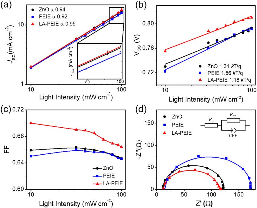
COMMUNICATIONS MATERIALS | https://doi.org/10.1038/s43246-021-00131-4                                                                   ARTICLE

between the bandgap (Eg) and actual VOC, Eg of 1.65 and 1.64 eV                Moreover, VOC can be represented as follows:
for PEIE and LA-PEIE, respectively, are obtained with a Tauc                                                       nkB T
plot, as shown in Fig. 2d. Notably, the VOC loss (Eg/q-VOC) of the                                    V OC ðIÞ ¼         lnðIÞ þ C                   ð1Þ
LA-PEIE is only 0.82 V, which is 0.04 V lower than that of the                                                       q
PEIE (0.86 V). This lower energy loss indicates a reduced                      where kB, T, and q are the Boltzmann constant, temperature, and
interfacial area for recombination in the LA-PEIE devices. The                 elemental charge, respectively; n and C represent the ideality
modification of PEIE with LA shifted its work function (WF)                     factor and a constant, respectively. The ideality factor n is
from 4.4 to 4.1 eV as shown in Fig. 2e, because the induced                    extracted from the slope of (1), giving 1.31, 1.56, and 1.18 for the
surface dipoles at the photoactive layer/cathode interface lower               ZnO, PEIE, and LA-PEIE CIL, respectively, as shown in Fig. 3b.
the electrostatic potential at the interface, which is evident from            These results signify that the OPV with LA-PEIE CIL has the
the energy band diagram (Fig. 2f). The low WF and enhanced                     lowest trap-assisted recombination due to the enhanced internal
interfacial dipoles of the LA-PEIE devices can also improve the                electric field and improved photoactive layer quality38,39,46–49.
quality of electrical contact by forming an Ohmic contact with the             The large difference in FF (Fig. 3c) at low light intensities can be
fullerene acceptor48,49. For comparison, the WF of ZnO is also                 ascribed to RSH and trap-assisted recombination, which shows
presented (4.3 eV). The better photoactive layer morphology of                 charge transport supporting capability of the LA-PEIE CIL53,54.
the LA-PEIE owing to its better affinity at the cathode/                        Moreover, the higher VOC and FF of the LA-PEIE CIL at low light
photoactive layer interface also aids in reducing the energy                   intensity can be beneficial for indoor applications under low-light
loss50,51. In contrast, the PEIE device has a higher energy barrier            intensity55,56.
to the lowest unoccupied molecular orbital (LUMO) acceptor,                       The interfacial charge transport properties of the OPVs can be
which enhances the surface recombination and decreases the                     easily determined via EIS. The OPV can be modeled with an
electric field, thereby reducing JSC and VOC52.                                 equivalent circuit of an internal series resistance (RS), a charge
                                                                               transport resistance (RCT), and a constant phase element (CPE)
                                                                               represents nonideal capacitor defined by interface capacitor
Charge carrier recombination dynamics. To elucidate the                        (CPE-T) and ideal capacitor (CPE-P)57 as shown in the inset of
charge recombination kinetics in the OPV devices: (i) the illu-                Fig. 3d. The parameters obtained from the fitting of the Nyquist
minated J–V characteristics were analyzed as a function of light               plot of EIS are summarized in Supplementary Table S4. In the
intensity, and (ii) electrochemical impedance spectroscopy (EIS)               Nyquist plot, the radius of the low-frequency semicircle
was performed. The J–V curves at different light intensities were              represents the resistance of the CIL. Thus, it can be inferred
measured and compared, as shown in Supplementary Fig. S5a–c,                   that a better carrier transport leads to a smaller value of RCT58.
for ZnO, PEIE, and LA-PEIE CILs. The PCE of OPV devices                        Figure 3d shows that LA-PEIE has the best charge transport
monotonically increases with lower light intensity, particularly for           properties for the interlayers of OPVs, with the RCT of 105.7 Ω
the LA-PEIE device (see Supplementary Fig. S5d). The power law                 cm2. Besides, the LA-PEIE also exhibits the smallest RS value
relates the JSC to the light intensity as JSC ∝ Iα, where I is the light       (13.75 Ω), indicating less recombination loss at the photoactive
intensity and the exponent α indicates bimolecular recombination               layer/cathode interface, leading to an increase in the FF and JSC of
coefficient. Therefore, α~1 implies a smaller recombination loss.               the devices59–62. The higher RS value of 19.97 Ω and higher RCT
In Fig. 3a, the α values are 0.94, 0.92, and 0.95 for the OPV                  (151.8 Ω cm2) for the PEIE CIL implies that the generated charges
devices with ZnO, PEIE, and LA-PEIE CIL, respectively.                         can accumulate at the photoactive layer/cathode interface owing

Fig. 3 Charge carrier recombination dynamics. a Light intensity dependent a JSC, b VOC and c FF of rigid OPV devices with various CILs. The straight line
represent the linear fitting. d EIS Nyquist plot of rigid OPV devices with ZnO (black solid circles), PEIE (blue solid squares), and LA-PEIE (red solid
triangles).

COMMUNICATIONS MATERIALS | (2021)2:26 | https://doi.org/10.1038/s43246-021-00131-4 | www.nature.com/commsmat                                           5
ARTICLE COMMUNICATIONS MATERIALS | https://doi.org/10.1038/s43246-021-00131-4
to the large mismatch between the energy levels of the opposed to its counterparts. The combined optical and electrical
photoactive layer and ITO substrate63–65. Since our photoactive improvements that are caused by the multifunctional fatty acid-
layer is very thin (~110 nm), the recombination capacitance modified PEIE increase the PCE. This occurrence happens when
becomes large. Therefore, the characteristic frequency of the the dipoles are aligned with the electric field, it can vibrate the
high-frequency circle in the Nyquist plot approaches that of the dipoles and impede the electric field, which is observed as an
low-frequency one, owing to which it is not observed separately. optical loss. In comparison with the disordered dipoles of the
The time-resolved photoluminescence (TRPL) decay character- PEIE, most dipoles of the LA-PEIE are relatively well aligned
ization for the PTB7-th:PC70BM active layer deposited on various normal to the surface (or aligned with the propagation direction
CILs were carried out to study the charge extraction. Supple- of light)70. It is observed that the optical loss of the LA-PEIE is
mentary Fig. S11 shows the TRPL curve (with an excitation at lower than that of the PEIE in Fig. 4d. Generally, metal oxides
405 nm and emission at 745 nm). The PL decay time and such as ZnO and TiOx are used as optical and mechanical
amplitudes are fitted and estimated using the double exponential spacers; however, these metal oxides are not used in flexible
function (Eq. (2)). electronic devices71–73. Thus, it is meaningful to design organic
interfacial materials with wettability driven adjustable optical and
f ðt Þ ¼ A1 expt=τ 1 þ A2 expt=τ 2 þ C ð2Þ electrical characteristics for developing flexible electronic devices.
where τ1 and τ2 are the fast and the slow decay times, respectively;
A1 and A2 are the pre-exponential constants or decay amplitudes; Photovoltaic performance of flexible OPVs. To understand the
C is a constant for the baseline offset66. The fitted parameters are applicability of various CILs in flexible OPVs, flexible OPV
tabulated in Supplementary Table S9. The τave is calculated by devices with an inverted structure were fabricated with PTB7-Th:
using Eq. (3). PC70BM photoactive layer. As shown in Fig. 5a and Table 1, the
LA-PEIE-based flexible device achieved a PCE of 9.04% with a
A1 τ 21 þ A2 τ 22 VOC of 0.80 V, JSC of 16.99 mA cm−2, and FF of 0.66. These
τ ave ¼ ð3Þ
A1 τ 1 þ A1 τ 1 values are superior to those of the ZnO and PEIE flexible devices,
which showed a PCE of 6.41% (VOC: 0.79 V, JSC: 15.28 mA cm−2,
The TRPL spectrum of the PTB7-th:PC70BM on the LA-PEIE
and FF: 0.53) and 7.87% (VOC: 0.76 V, JSC: 15.53 mA cm−2, and
shows a decay time of 0.53 ns, which is smaller than the decay
FF: 0.64), respectively. Here, the S-shaped behavior of the ZnO
time of 1.08 ns of the pristine PEIE. Compared with the PEIE, the
CIL OPV device indicates the non-compatibility of metal oxide
shorter decay time of the LA-PEIE-based implies that the electron
CILs with flexible substrates. Organic CILs, especially bifacial
extraction at the LA-PEIE/active layer interface is more efficient
interlayer-designed organic CILs, play a highly decisive role in
than that at the PEIE/active layer interface67–69. The improved
flexible OPVs. The EQE spectra of the flexible devices are shown
charge extraction characteristic is confirmed via photoconductive
in Fig. 5b. The flexible devices have low EQE values in the UV
atomic force microscopy. The illumination intensity-dependent
region owing to the UV light absorption characteristic of the PEN
photocurrent and mapped images of the PEIE and LA-PEIE CILs
substrate.
on the ITO glass substrates are shown in Supplementary Fig. S6a,
b, and the average local photocurrents are given in Supplemen-
tary Table S6. The average of photocurrent with respect to light Bending and air-storage stability test of flexible OPVs. The
intensity is illustrated in Supplementary Fig. S6c. The LA-PEIE interfacial contact can also influence the mechanical stability of
CIL exhibited higher local photocurrents under all illuminations flexible OPVs. Figure 5c shows the PCE of the flexible OPVs with
compared to the PEIE CIL, implying that LA-PEIE is more ZnO, PEIE, and LA-PEIE CILs that were measured after the
efficient in charge extraction at the cathode interface. bending test for up to 200 cycles with different bending radii. The
OPV with the LA-PEIE CIL was maintained at 95.83% of its
Estimating optical loss in CILs. The drastically enhanced device initial PCE value, which was higher than that (82.21%) of the
characteristics due to the modification of PEIE CIL, particularly device with PEIE CIL; however, the performance of the OPV with
the value of JSC, cannot be fully understood by the improved the ZnO CIL severely deteriorated, even at a bending radius of
electrical properties, such as reduced charge recombination, 0.75 cm. The degradation by bending the device is believed to
increased charge extraction, and energy balance. In addition, the increase the sheet resistance due to the cracks on the ITO sub-
optical properties of the PEIE and LA-PEIE CIL were further strate and delamination of the photoactive layer/ITO74–76. In
investigated using the scattering matrix method, as shown in addition, when the flexible OPVs were exposed to air without any
Fig. 4, although it was mentioned earlier that the optical trans- encapsulation, the ones with LA-PEIE CIL exhibited superior
mittances of the two samples were almost identical. The trans- stability (Fig. 5d). The other parameters are shown in Supple-
mittance and reflectance were measured for the single layer of the mentary Fig. S7a–c. The LA-PEIE device retained 87.75% of its
PEIE (50 nm), LA-PEIE (50 nm), and photoactive layer (110 nm) initial PCE after 10 days; however, the PCE of the ZnO and PEIE
on a glass substrate, and the optical parameters (refractive index, devices decreased to 38.80% and 77.43% of their initial values,
n and extinction coefficient, k) of each layer were extracted, as respectively. The decrease in PCE is mainly influenced by a
shown in Fig. 4a. As can be seen, the k curve of the LA-PEIE is decrease in FF. The modification of PEIE by the LA hydrophobic
formed below that of the PEIE, an observation that is consistent molecule is believed to improve the adhesion of the active layer
with the bandgap energy of each layer obtained with the Tauc for effectively preventing the penetration of moisture to the gap
plots in Fig. 2d. Using the optical parameters, optical simulation between the photoactive layer and cathode of the device.
of the OPVs were performed with the structure of glass/ITO (150
nm)/PEIE or LA-PEIE (5 nm)/photoactive (110)/MoO (5 nm)/ Large-area flexible OPV modules. For practical applications, a
Ag. In Fig. 4b, the EQE of the OPV with the LA-PEIE CIL is large-area device applicability test is crucial. Sub-module-sized
slightly higher than that with the PEIE CIL, while the reflectance OPV devices were fabricated on a 5 × 7 cm2 (9 cells) PEN flexible
(Fig. 4c) of the two OPVs is almost the same. This is because the substrate with an active area of 18.63 cm2 and its device structure
optical loss in the LA-PEIE is lower than that in the PEIE, as seen is shown in Supplementary Fig. S8a. The J–V curves of flexible
from Fig. 4d. The optical simulation clearly shows that LA-PEIE OPV sub-modules with PEIE and LA-PEIE CILs are shown in
can act as a molecular optical spacer and results in a higher JSC, as Supplementary Fig. S8b, and the photovoltaic properties are
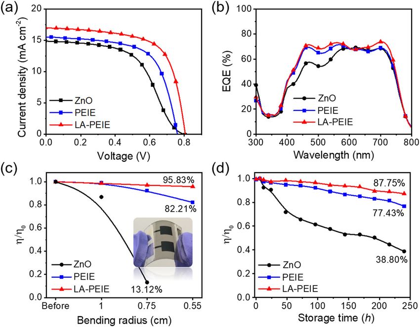
6 COMMUNICATIONS MATERIALS | (2021)2:26 | https://doi.org/10.1038/s43246-021-00131-4 | www.nature.com/commsmatCOMMUNICATIONS MATERIALS | https://doi.org/10.1038/s43246-021-00131-4 ARTICLE Fig. 4 Estimation of optical losses. The Optical simulation for the OPVs with the PEIE (blue line) and LA-PEIE (red line): a refractive index (n) and extinction coefficient (k), b simulated external quantum efficiency (EQE), c reflectance, and d calculated optical loss in CILs. Fig. 5 Photovoltaics performance and stability of flexible OPVs. a Current density–voltage characteristics, b EQE spectra, c normalized PCE of 200 bending cycles with respect to substrate bending radius, and d normalized stability graph of flexible OPVs with ZnO (black line, solid circles), PEIE (blue line, solid square), and LA-PEIE (red line, solid triangles) CILs. summarized in Supplementary Table S7. The OPV module with Device performance of the flexible OLEDs. Finally, to verify the LA-PEIE CIL exhibited the highest PCE of 8.31% (FF: 0.59, JSC: effect of LA-PEIE CIL on the performance of the OLEDs, 2.04 mA cm−2, and VOC: 6.88 V), while the module with PEIE solution-processed OLEDs were fabricated using ZnO, PEIE, and CIL showed a PCE of 6.41% only (FF: 0.55, JSC: 1.78 mA cm−2 LA-PEIE CILs. The structure of the fabricated OLED is shown in and VOC: 6.51 V). The enhanced performance is more pro- Supplementary Fig. S9a. The current density–voltage–luminance nounced for all the factors. Based on this, one can strongly argue (J–V–L) characteristics of the OLEDs that were fabricated on that fatty acid-modified PEIE is a suitable interfacial material for flexible substrates with different CILs are shown in Supplemen- the realization of flexible and large-area OPV modules. tary Figure S9c–e. The devices with LA-PEIE showed higher COMMUNICATIONS MATERIALS | (2021)2:26 | https://doi.org/10.1038/s43246-021-00131-4 | www.nature.com/commsmat 7
ARTICLE                                                             COMMUNICATIONS MATERIALS | https://doi.org/10.1038/s43246-021-00131-4

current densities and luminescence when compared to the                     Methods
reference devices based on PEIE. The LA-PEIE-based OLED                     Materials. PEIE, ethanol, methanol, chlorobenzene, and DIO were purchased from
exhibited a notably reduced driving voltage (3.2 V at 150 cd m−2)           Sigma-Aldrich. Linoleic acid (Merck KGaA), PTB7-Th (1-materials), PC70BM
                                                                            (Merck KGaA), PEDOT:PSS (AI4083, Heraeus), and (PDY-132, Merck KGaA)
as compared to the PEIE-based OLED (3.4 V at 150 cd m−2). The               were purchased commercially. All the materials were used without any further
LA-PEIE CIL forms strong interfacial dipoles at the interface of            purification.
the emissive layers and cathodes. The presence of these dipoles
can reduce the electron injection barrier at the interface and              Solar cell fabrication. The chemical structures of the materials that were used in
enhance the electron injection property, which returns to a low             this study are shown in Supplementary Fig. S1. PEIE and LA-PEIE solutions were
on-set voltage. Moreover, LA-PEIE creates hydrophobic interac-              prepared by dissolving PEIE (20 mg) in ethanol (10 mL). For LA-PEIE, the linoleic
                                                                            acid solution, dissolved in methanol, was added to the PEIE solution and stirred
tions that are favorable for coating the emissive layer uniformly to        overnight. Before using, PEIE and LA-PEIE were filtered through a 0.5 μm poly-
ensure improved contact at the interface. Therefore, the highest            vinylidene fluoride filter. The active layer solution was prepared by dissolving
current efficiency (CE) and power efficiency (PE) for the lumi-               PTB7-Th (10 mg mL−1) and PC70BM (18 mg mL−1) in chlorobenzene (0.97 mL)
nescence were obtained for the flexible OLED with the LA-PEIE                and 1,8-diiodooctane (0.03 mL). The solution was stirred overnight at 70 °C, and
                                                                            then the solution was filtered using a 0.45 μm polytetrafluoroethylene filter. The
CIL, as shown in Supplementary Fig. S9b and Supplementary                   patterned ITO/glass substrates were cleaned sequentially with deionized water,
Table S8. The maximum CE and PE were 10.21 cd A−1 and 8.47                  acetone, and isopropanol for 10 min each. Patterned ITO or PEN substrates were
lm W−1, respectively. The excellent charge injection characteristic         used without the cleaning process. The ITO substrates were treated with UV–ozone
of the LA-PEIE CIL contributed towards making the LA-PEIE-                  plasma for 1000 s and transferred to an Ar-filled glove box. The ultra-thin PEIE
                                                                            and LA-PEIE CIL were spin-coated using 100 μL of PEIE or LA-PEIE solution on
based OLED superior to the other CIL-based OLEDs. The pre-                  the ITO substrates at 2000 rpm for 60 s (the thickness of PEIE and LA-PEIE is ~5
viously mentioned distinguishing features of the LA-PEIE CIL                nm). These devices were dried at room temperature for 15 min. The active layer
allow the fabrication of low-cost, long-lived, large area, and highly       was spin-coated using a blend solution at 2000 rpm for 40 s and then dried for 3 h.
efficient solution-processed OLEDs with the conventional device              The methanol treatment was performed at 2000 rpm for 40 s to remove the DIO in
                                                                            the photoactive layer. Finally, MoO3 (7 nm) and Ag (100 nm) were thermally
architecture. Owing to such excellent features, these solution-             evaporated in a vacuum chamber (chamber pressure
COMMUNICATIONS MATERIALS | https://doi.org/10.1038/s43246-021-00131-4 ARTICLE
Received: 30 October 2020; Accepted: 4 February 2021; 30. Zhang, Z. et al. Polymer with a 3D conductive network: a thickness-insensitive
electron transport layer for inverted polymer solar cells. J. Mater. Chem. A 6,
12969–12973 (2018).
31. Borse, K., Sharma, R., Gupta, D. & Yella, A. Interface engineering through
electron transport layer modification for high efficiency organic solar cells.
References RSC Adv. 8, 5984–5991 (2018).
1. Kippelen, B. & Brédas, J.-L. Organic photovoltaics. Energy Environ. Sci. 2, 251 32. Zhang, Z. et al. Non-conjugated polymers as thickness-insensitive electron
(2009). transport materials in high-performance inverted organic solar cells. J. Energy
2. Xia, Y., Xu, X. & Inganäs, O. Photovoltage loss in semi-transparent organic Chem. 47, 196–202 (2020).
photovoltaic devices. Org. Electron. 74, 37–40 (2019). 33. Ohisa, S., Suzuki, M., Chiba, T. & Kido, J. Doping of tetraalkylammonium
3. Krebs, F. C., Tromholt, T. & Jørgensen, M. Upscaling of polymer solar cell salts in polyethylenimine ethoxylated for efficient electron injection layers in
fabrication using full roll-to-roll processing. Nanoscale 2, 873–886 (2010). solution-processed organic light-emitting devices. ACS Appl. Mater. Interfaces
4. Ma, X. et al. Simultaneously improved efficiency and average visible 11, 25351–25357 (2019).
transmittance of semitransparent polymer solar cells with two ultra-narrow 34. Kang, Q. et al. A printable organic cathode interlayer enables over 13%
bandgap nonfullerene acceptors. J. Mater. Chem. A 6, 21485–21492 (2018). efficiency for 1-cm2 organic solar cells. Joule 3, 227–239 (2019).
5. Salehi, A., Fu, X., Shin, D.-H. & So, F. Recent advances in OLED optical 35. Ma, Z. et al. Influences of surface roughness of ZnO electron transport layer
design. Adv. Funct. Mater. 29, 1808803 (2019). on the photovoltaic performance of organic inverted solar cells. J. Phys. Chem.
6. Tao, J. et al. Highly transparent, highly thermally stable nanocellulose/polymer C 116, 24462–24468 (2012).
hybrid substrates for flexible OLED devices. ACS Appl. Mater. Interfaces 12, 36. Wang, Z. et al. Urea-doped ZnO films as the electron transport layer for high
9701–9709 (2020). efficiency inverted polymer solar cells. Front. Chem. 6, 398 (2018).
7. MacDonald, W. A. et al. Latest advances in substrates for flexible electronics. J. 37. Xiao, B., Wu, H. & Cao, Y. Solution-processed cathode interfacial layer materials
Soc. Inf. Disp. 15, 1075–1083 (2007). for high-efficiency polymer solar cells. Mater. Today 18, 385–394 (2015).
8. Cui, Y. et al. Efficient semitransparent organic solar cells with tunable color 38. Lim, D. C. et al. Spontaneous formation of nanoripples on the surface of ZnO
enabled by an ultralow-bandgap nonfullerene acceptor. Adv. Mater. 29, thin films as hole-blocking layer of inverted organic solar cells. Sol. Energy
1527–1538 (2017). Mater. Sol. Cells 95, 3036–3040 (2011).
9. Lee, H. et al. Color-tunable organic light-emitting diodes with vertically 39. Yuan, K., Chen, L., Li, F. & Chen, Y. Nanostructured hybrid ZnO@CdS
stacked blue, green, and red colors for lighting and display applications. Opt. nanowalls grown in situ for inverted polymer solar cells. J. Mater. Chem. C 2,
Express 26, 18351–18361 (2018). 1018–1027 (2014).
10. Liu, Q. et al. 18% Efficiency organic solar cells. Sci. Bull. 65, 272–275 (2020). 40. Chang, C.-Y., Tsai, B.-C., Lin, M.-Z., Huang, Y.-C. & Tsao, C.-S. An integrated
11. Fonrodona, M. et al. PEN as substrate for new solar cell technologies. Sol. approach towards the fabrication of highly efficient and long-term stable
Energy Mater. Sol. Cells 89, 37–47 (2005). perovskite nanowire solar cells. J. Mater. Chem. A 5, 22824–22833 (2017).
12. Lee, U. J. et al. Surface interpenetration between conducting polymer and PET 41. Rana, V., Cañamares, M. V., Kubic, T., Leona, M. & Lombardi, J. R. Surface-
substrate for mechanically reinforced ITO-free flexible organic solar cells. Sol. enhanced Raman spectroscopy for trace identification of controlled substances:
Energy Mater. Sol. Cells 108, 50–56 (2013). morphine, codeine, and hydrocodone. J. Forensic Sci. 56, 200–207 (2011).
13. Huang, J., Yin, Z. & Zheng, Q. Applications of ZnO in organic and hybrid 42. Wang, M., Shi, G., Zhu, Y., Wang, Y. & Ma, W. Au-decorated dragonfly wing
solar cells. Energy Environ. Sci. 4, 3861–3877 (2011). bioscaffold arrays as flexible surface-enhanced Raman scattering (SERS)
14. Xiong, S. et al. 12.5% flexible nonfullerene solar cells by passivating the substrate for simultaneous determination of pesticide residues. Nanomaterials
chemical interaction between the active layer and polymer interfacial layer. 8, 289 (2018).
Adv. Mater. 31, 1806616 (2019). 43. Ghazvini, M. S., Pulletikurthi, G., Lahiri, A. & Endres, F. Electrochemical and
15. Kumar, M. H. et al. Flexible, low-temperature, solution processed ZnO-based spectroscopic studies of zinc acetate in 1-ethyl-3-methylimidazolium acetate
perovskite solid state solar cells. Chem. Commun. 49, 11089 (2013). for zinc electrodeposition. ChemElectroChem 3, 598–604 (2016).
16. Qiu, X. et al. Efficient, stable and flexible perovskite solar cells using two-step 44. Tu, J.-S., Perevedentseva, E., Chung, P.-H. & Cheng, C.-L. Size-dependent
solution-processed SnO2 layers as electron-transport-material. Org. Electron. surface CO stretching frequency investigations on nanodiamond particles. J.
58, 126–132 (2018). Chem. Phys. 125, 174713 (2006).
17. Al-hashimi, M. K., Kadem, B. Y. & Hassan, A. K. Rutile TiO2 films as electron 45. Petit, T. et al. Unusual water hydrogen bond network around hydrogenated
transport layer in inverted organic solar cell. J. Mater. Sci. Mater. Electron 29, nanodiamonds. J. Phys. Chem. C 121, 5185–5194 (2017).
7152–7160 (2018). 46. Selvarajan, P. et al. Potential of Raman spectroscopy towards understanding structures
18. Nho, S. et al. Highly efficient inverted bulk-heterojunction solar cells with a of carbon-based materials and perovskites. Emergent Mater. 2, 417–439 (2019).
gradiently-doped ZnO layer. Energy Environ. Sci. 9, 240–246 (2016). 47. Proctor, C. M. & Nguyen, T.-Q. Effect of leakage current and shunt resistance
19. Wu, Z., Yu, H., Shi, S. & Li, Y. Bismuth oxysulfide modified ZnO nanorod on the light intensity dependence of organic solar cells. Appl. Phys. Lett. 106,
arrays as an efficient electron transport layer for inverted polymer solar cells. J. 83301 (2015).
Mater. Chem. A 7, 14776–14789 (2019). 48. Cai, Y. et al. Novel nonconjugated polymer as cathode buffer layer for efficient
20. Huang, X., Yu, H., Shi, S. & Huang, C. Improving the performance of inverted organic solar cells. ACS Appl. Mater. Interfaces 10, 24082–24089 (2018).
polymer solar cells by the efficiently doping and modification of electron 49. Brabec, C. J. et al. Origin of the open circuit voltage of plastic solar cells. Adv.
transport layer-ZnO. Org. Electron. 65, 311–320 (2019). Funct. Mater. 11, 374–380 (2001).
21. He, Z. et al. Largely enhanced efficiency with a PFN/Al bilayer cathode in high 50. Mihailetchi, V. D., Blom, P. W. M., Hummelen, J. C. & Rispens, M. T.
efficiency bulk heterojunction photovoltaic cells with a low bandgap Cathode dependence of the open-circuit voltage of polymer:fullerene bulk
polycarbazole donor. Adv. Mater. 23, 3086–3089 (2011). heterojunction solar cells. J. Appl. Phys. 94, 6849–6854 (2003).
22. Zhao, Y. et al. Enhanced charge collection in polymer photovoltaic cells by 51. Tang, Z. et al. Relating open-circuit voltage losses to the active layer morphology and
using an ethanol-soluble conjugated polyfluorene as cathode buffer layer. Sol. contact selectivity in organic solar cells. J. Mater. Chem. A 6, 12574–12581 (2018).
Energy Mater. Sol. Cells 93, 604–608 (2009). 52. Menke, S. M., Ran, N. A., Bazan, G. C. & Friend, R. H. Understanding energy
23. Na, S.-I., Oh, S.-H., Kim, S.-S. & Kim, D.-Y. Efficient organic solar cells with loss in organic solar cells: toward a new efficiency regime. Joule 2, 25–35 (2018).
polyfluorene derivatives as a cathode interfacial layer. Org. Electron. 10, 53. Proctor, C. M., Kuik, M. & Nguyen, T.-Q. Charge carrier recombination in
496–500 (2009). organic solar cells. Prog. Polym. Sci. 38, 1941–1960 (2013).
24. Lozano-Hernández, L. A. et al. Structurally simple OLEDs based on a new 54. Sherkar, T. S., Momblona, C., Gil-Escrig, L., Bolink, H. J. & Koster, L. J. A.
fluorinated poly(oxindolylidenearylene). Dye. Pigment. 173, 107989 (2020). Improving perovskite solar cells: insights from a validated device model. Adv.
25. Wu, Y., Liu, Y., Emrick, T. & Russell, T. P. Polymer design to promote low Energy Mater. 7, 1602432 (2017).
work function surfaces in organic electronics. Prog. Polym. Sci. 103, 101222 55. Jahandar, M. et al. High-performance CH3NH3PbI3-inverted planar
(2020). perovskite solar cells with fill factor over 83% via excess organic/inorganic
26. Zhou, Y. et al. A universal method to produce low-work function electrodes halide. ACS Appl. Mater. Interfaces 9, 35871–35879 (2017).
for organic electronics. Science (80-.) 336, 327–332 (2012). 56. Cojocaru, L. et al. Determination of unique power conversion efficiency of
27. Yu, H., Huang, X. & Huang, C. PEIE doped ZnO as a tunable cathode solar cell showing hysteresis in the I-V curve under various light intensities.
interlayer for efficient polymer solar cells. Appl. Surf. Sci. 470, 318–330 (2019). Sci. Rep. 7, 11790 (2017).
28. Yeo, J.-S. et al. In-depth considerations for better polyelectrolytes as interfacial 57. Cowan, S. R., Roy, A. & Heeger, A. J. Recombination in polymer-fullerene
materials in polymer solar cells. Nano Energy 21, 26–38 (2016). bulk heterojunction solar cells. Phys. Rev. B 82, 245207 (2010).
29. Kim, Y.-H. et al. Polyethylene imine as an ideal interlayer for highly efficient 58. Zhou, P. et al. Nonconjugated polymer poly(vinylpyrrolidone) as an efficient
inverted polymer light-emitting diodes. Adv. Funct. Mater. 24, 3808–3814 interlayer promoting electron transport for perovskite solar cells. ACS Appl.
(2014). Mater. Interfaces 9, 32957–32964 (2017).
COMMUNICATIONS MATERIALS | (2021)2:26 | https://doi.org/10.1038/s43246-021-00131-4 | www.nature.com/commsmat 9ARTICLE COMMUNICATIONS MATERIALS | https://doi.org/10.1038/s43246-021-00131-4
59. Pockett, A., Lee, H. K. H., Coles, B. L., Tsoi, W. C. & Carnie, M. J. A combined Acknowledgements
transient photovoltage and impedance spectroscopy approach for a This research was supported by Korea Institute of Materials Science (KIMS, No.
comprehensive study of interlayer degradation in non-fullerene acceptor PNK7660), Korea Institute of Energy Technology Evaluation and Planning (KETEP, No.
organic solar cells. Nanoscale 11, 10872–10883 (2019). 2018201010636A) and the National Research Foundation of Korea (NRF
60. Li, Z. et al. Impedance investigation of the highly efficient polymer solar cells 2020M3H4A3081820).
with composite CuBr2/MoO3 hole transport layer. Phys. Chem. Chem. Phys.
19, 20839–20846 (2017).
61. von Hauff, E. Impedance spectroscopy for emerging photovoltaics. J. Phys.
Author contributions
S.K., and A.P., contributed equally to this work. D.C.L., conceived the idea. M.J., and D.C.
Chem. C 123, 11329–11346 (2019).
L., designed the experiment. S.K., conducted most of the OPV device fabrications and
62. Rasool, S. et al. Amine-based interfacial engineering in solution-processed
characterizations. A.P., fabricated the large-area OPV devices, conducted charge carrier
organic and perovskite solar cells. ACS Appl. Mater. Interfaces 11,
recombination analysis and stability test. J.W.H., J.H.K., and Y.H.K., carried out the
16785–16794 (2019).
OLED device and characterization. Y.K., and M.S., design and conduct the simulations. J.
63. Kim, S. et al. The role of cation and anion dopant incorporated into a ZnO
H., conducted the film morphology. S.C., carried out spectroscopy measurements. M.S.,
electron transporting layer for polymer bulk heterojunction solar cells. RSC
Y.H.K., M.J., and D.C.L., wrote the manuscript. All authors discussed the results and
Adv. 9, 37714–37723 (2019).
commented on the manuscript.
64. Wetzelaer, G.-J. A. H., Koster, L. J. A. & Blom, P. W. M. Bimolecular and trap-
assisted recombination in organic bulk heterojunction solar cells. Org.
Photovolt. 343–376, https://doi.org/10.1002/9783527656912.ch11 (2014). Competing interests
65. Lee, J.-H. et al. Reinforcing the built-in field for efficient charge collection in The authors declare no competing interests.
polymer solar cells. Adv. Funct. Mater. 28, 1705079 (2018).
66. Sundqvist, A., Sandberg, O. J., Nyman, M., Smått, J.-H. & Österbacka, R.
Origin of the S-shaped JV curve and the light-soaking issue in inverted Additional information
organic solar cells. Adv. Energy Mater. 6, 1502265 (2016). Supplementary information The online version contains supplementary material
67. Cai, Q. et al. Enhancing efficiency of planar structure perovskite solar cells available at https://doi.org/10.1038/s43246-021-00131-4.
using Sn-doped TiO2 as electron transport layer at low temperature.
Electrochim. Acta 261, 227–235 (2018). Correspondence and requests for materials should be addressed to M.J. or D.C.L.
68. Zhong, D. et al. Synthesis of oriented TiO2 nanocones with fast charge transfer
for perovskite solar cells. Nano Energy 11, 409–418 (2015). Peer review information Primary handling editor: John Plummer
69. Tian, C. et al. A C60 modification layer using a scalable deposition technology
for efficient printable mesoscopic perovskite solar cells. Sol. RRL 2, 1800174 Reprints and permission information is available at http://www.nature.com/reprints
(2018).
70. Baloch, A. A. B. et al. Analysis of photocarrier dynamics at interfaces in Publisher’s note Springer Nature remains neutral with regard to jurisdictional claims in
perovskite solar cells by time-resolved photoluminescence. J. Phys. Chem. C published maps and institutional affiliations.
122, 26805–26815 (2018).
71. Rosell, F. I. & Boxer, S. G. Polarized absorption spectra of green fluorescent
protein single crystals: transition dipole moment directions. Biochemistry 42, Open Access This article is licensed under a Creative Commons
177–183 (2003). Attribution 4.0 International License, which permits use, sharing,
72. Park, S. H. et al. Bulk heterojunction solar cells with internal quantum adaptation, distribution and reproduction in any medium or format, as long as you give
efficiency approaching 100%. Nat. Photonics 3, 297–302 (2009). appropriate credit to the original author(s) and the source, provide a link to the Creative
73. Lee, J. K. et al. Efficacy of TiOx optical spacer in bulk-heterojunction solar cells Commons license, and indicate if changes were made. The images or other third party
processed with 1,8-octanedithiol. Appl. Phys. Lett. 92, 243308 (2008). material in this article are included in the article’s Creative Commons license, unless
74. Kyaw, A. K. K. et al. Improved light harvesting and improved efficiency by indicated otherwise in a credit line to the material. If material is not included in the
insertion of an optical spacer (ZnO) in solution-processed small-molecule article’s Creative Commons license and your intended use is not permitted by statutory
solar cells. Nano Lett. 13, 3796–3801 (2013). regulation or exceeds the permitted use, you will need to obtain permission directly from
75. Li, Y., Xu, G., Cui, C. & Li, Y. Flexible and semitransparent organic solar cells. the copyright holder. To view a copy of this license, visit http://creativecommons.org/
Adv. Energy Mater. 1701791 (2018). licenses/by/4.0/.
76. Hashemi, S. A., Ramakrishna, S. & Aberle, A. G. Recent progress in
flexible–wearable solar cells for self-powered electronic devices. Energy
Environ. Sci. 13, 685–743 (2020). © The Author(s) 2021
10 COMMUNICATIONS MATERIALS | (2021)2:26 | https://doi.org/10.1038/s43246-021-00131-4 | www.nature.com/commsmatYou can also read