THE EVOLUTION OF ENTERPRISE STORAGE - Bruce Yellin - Dell EMC ...
←
→
Page content transcription
If your browser does not render page correctly, please read the page content below

THE EVOLUTION OF ENTERPRISE
STORAGE

Bruce Yellin
Bruceyellin@Yahoo.com

Knowledge Sharing Article
© 2020 Dell Inc. or its subsidiaries.

The Dell Technologies Proven Professional Certification program validates a wide range of skills
and competencies across multiple technologies and products.

From Associate, entry-level courses to Expert-level, experience-based exams, all professionals
in or looking to begin a career in IT benefit from industry-leading training and certification paths
from one of the world’s most trusted technology partners.

Proven Professional certifications include:

 • Cloud
 • Converged/Hyperconverged Infrastructure
 • Data Protection
 • Data Science
 • Networking
 • Security
 • Servers
 • Storage
 • Enterprise Architect

Courses are offered to meet different learning styles and schedules, including self-paced On
Demand, remote-based Virtual Instructor-Led and in-person Classrooms.

Whether you are an experienced IT professional or just getting started, Dell Technologies
Proven Professional certifications are designed to clearly signal proficiency to colleagues and
employers.

Learn more at www.dell.com/certification

2020 Dell Technologies Proven Professional Knowledge Sharing 2
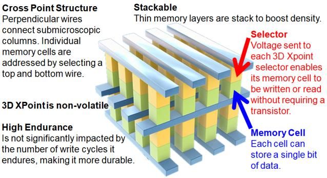
Table of Contents
Everything Must Change ............................................................................................................ 4

 Hard Drives Losing Ground to Solid-State Drives ................................................................... 5

 New Shapes ........................................................................................................................... 6

 New Interfaces ....................................................................................................................... 8

How Do SSDs Work? ................................................................................................................12

 Anatomy of a READ ..............................................................................................................13

 What is a Cell? ......................................................................................................................14

Enter Quadruple-Level Cell SSDs .............................................................................................15

 Quad-Level Cells look like an easy concept, but are they? ....................................................16

 The Big Paradigm Shift – Multi-Level NAND Cells .................................................................17

 Endurance Is a Big Question .................................................................................................18

 Understanding QLC Data Profiles - What Workloads Work Best? .........................................20

Intel Optane ..............................................................................................................................21

What’s new in storage? .............................................................................................................22

 NVMe and Just a Bunch of Flash ..........................................................................................22

 NVMe Over Fabrics ...............................................................................................................23

 A New Bottleneck – The Network ..........................................................................................24

 Software-Defined Storage .....................................................................................................26

 SAS-4 ....................................................................................................................................28

 Storage Lifecycle Automation – Rebalancing SSD-based Storage ........................................29

 Storage Class Memory ..........................................................................................................30

Conclusion ................................................................................................................................31

Footnotes ..................................................................................................................................33

Disclaimer: The views, processes or methodologies published in this article are those of the
author. They do not necessarily reflect Dell Technologies’ views, processes or methodologies.

Dell.com/certification 3
Everything Must Change
Twenty years ago, Windows 98 pulsed through high-end 500MHz Pentium PCs with 64MB of
memory and a 10GB hard drive.1 Companies built three-tier architectures of servers, a gigabit
Fibre Channel Storage Area Network (SAN), and a “star-wars” looking EMC Symmetrix
8430 machine with dozens of 36GB Small Computer System Interface (SCSI) hard
drives. The 32GB cache array maxed out at 3½TB of storage and allowed access to
data in cache or a much slower hard drive layer. Storage engineers designed solutions
by adding up workloads and dividing by drive capacity and Input/output Operations Per
Second (IOPs), often over-designing them to meet workload peaks. Customers flocked to SANs
instead of server-based Direct-Attached Storage (DAS) to increase utilization, reduce costs, and
improve manageability and scalability. The enterprise storage world loved it!

A decade later, Windows XP used a 1.7GHz Pentium 4 PC, 80GB drive and 256MB of
memory.2 Companies upgraded their SAN to 4Gb/s and
a behemoth 10 ton, 9 rack DMX-4 with 2,400 hard drives
for 2PB of storage.3 A revolutionary hard drive shaped
73GB SCSI Solid-State Drive (SSD) dramatically boosted drive-resident application
performance. Each $18,000 SSD, which was comparable in performance to today’s small USB
flash drive, lacked the capacity and proved too expensive to replace spinning disks.4,5

Today, a Windows 10 PC runs on a 16GB 8-core processor at 3.6GHz with a 1TB SSD. On the
SAN-side, data center modernization and transformation can leverage a two rack, 4PB
PowerMax with a streamlined massively parallel protocol and interconnect for Storage
Class Memory (SCM) and Non-Volatile Memory Express (NVMe) SSDs. Engineers
now leverage platforms with 50% more performance than the previous generation and
trim costs by sizing solutions based on effective deduplication rates. IOP performance and
workload peaks are automatically handled.6,7 Can we possibly process data any faster?

While SANs are still popular, the twenty-year-old movement that freed storage from servers is
starting to come full circle. Virtualized multicore processors with fast interconnects have led
some customers to innovative x86 Hyperconverged Infrastructures (HCI) and Software-Defined
Storage (SDS) rather than older three-tier architectures. SAN features of file, block, and object
protocols, clones and snapshots, encryption, compression/deduplication, and replication are no
longer exclusive. SDS storage architecture can lower operational and capital expenses that

2020 Dell Technologies Proven Professional Knowledge Sharing 4
challenge today’s IT budgets. These new solutions incorporate SSDs in all sorts of packaging to
revolutionize enterprise storage designs.

Our innovative world is full of change. From a technology perspective, while hard drives,
mainframes, and magnetic tapes are still in use, the pace of change has increased. Similar
capacity and performance of a high-end circa 2000 Symmetrix can be found in an enterprise
server at a fraction of the cost. Just 6 layers of a 96-layer NOT AND (NAND) logic gate chip can
hold the contents of a large 10TB hard drive.8 (NAND chips are SSD building blocks and
covered in detail later on.)

Computer storage is on the precipice of yet another shift. Moore’s Law is being kept alive with
new types of storage that doubles the performance while halving the cost. The enterprise
storage world is constantly evolving and this paper is about those elements of change.

Hard Drives Losing Ground to Solid-State Drives
The annual hard drive unit growth rate is in decline. Worldwide hard drive
shipments slipped 2.5% annually from a 370 million unit peak in 2018 to
330 million in 2021. Meanwhile, SSD shipments increased 13% annually to
360 million units.9 High performing 15K RPM hard drives hold 900GB
while large capacity 20TB hard drives run at 7,200 RPM, both smaller and
slower than large high-performance SSDs.10,11 Systems needing fast response and high transfer
rates now use SSDs instead of 10K-15K RPM drives while applications such as video
surveillance still use lower-performing, lower cost 5,400-7,200 RPM units.12 While the market for
older hard drive technology is shrinking, 240 exabytes of rotating platters shipped in Q3 2019.

A decade ago, some programs that used four hard drives for capacity
now use one high density, high throughput dual actuator Heat Assisted
Magnetic Recording (HAMR) 20TB drive as shown to the right. Two
active heads double the IOPS and performance to 480MB/s for less
critical applications and high-performance secondary workloads. Seagate is planning a new
100TB HAMR drive for 2025.13,14

Just two decades ago, a $500,000 storage rack held a few terabytes of data. Concurrent access
was limited to a handful of small SCSI hard drives while consuming many kilowatts of power
and dissipating thousands of BTUs of heat. SSD innovations such as Triple-Level Cell (TLC)
with a 128-layer 1Tb die (a rectangular integrated circuit sliced from a circular wafer) are
happening faster than hard drive improvements. Breakthroughs with lower cost 144-layer Quad-

Dell.com/certification 5
Level Cell (QLC) 2½” SSDs and future 176-layer QLC SSDs could yield a 120TB hard drive
form factor.15,16 Without a rotating platter, SSDs can take on different shapes, allowing thirty-two
170TB SSDs with a new shape to deliver 5PB of storage in a 1U server or 217PB in a full rack.
This density/performance improvement helps close the SSD/hard drive price gap.

Motorized hard drives limit performance. I/O commands queued against fragmented data
experience higher latency due to increased head movement and rotational delay, resulting in
fewer IOPS and lower throughput. Latency, similar to the occasional lag between a TV video
and voice, critically represents the delay in programs getting I/O responses. Amazon equates
100ms of latency with a 1% web sale loss.17 SSDs do not have mechanical issues and easily
handle parallel low latency commands, making them ideal replacements for aging hard drives.

Lastly, hard drives seem to fail at a higher rate than their counterparts, although it is worth
noting that SSDs also wear out as we will discuss. The idea of critical components wearing out
is not new; after all, our cars have a spare tire for a reason.

New Shapes
It helped early SSD product adoption to use the familiar 2½” rectangular hard drive shape and fit
into existing drive slots. They used the same interface such as
SCSI (introduced in 1981), Serial Advanced Technology
Attachment (SATA), Serial Attached SCSI (SAS), and Peripheral
Component Interconnect Express (PCIe).18 This illustration shows
the shape of a 2½” QLC SSD is identical to a SCSI hard drive.

A U.2 drive represents the next phase of hot-swappable SSDs using a hard drive shape. It uses
the same SAS/SATA connector although the pinouts carry different signals19. Whereas the
SAS/SATA connector maps to a drive controller which then interfaces with PCIe, U.2 drives do
not require a controller and use the connector to map directly to a PCIe connection.

M.2 SSD cards were originally called Next Generation Form Factor (NGFF). The M.2 2280
(22mm x 80mm) is the size of a pack of chewing gum. Unlike
 .87”
2½” enterprise SSDs, M.2 is not “hot” replaceable. They require
 3.15”
the computer to be turned off since they plug into a dedicated
motherboard slot (or PCIe adapter card) and are not inserted
from the front of the machine. The cards scale up to 2TB of
capacity and lack a protective case. With the same general SSD circuitry but in a narrow form
factor, they are available with a SATA or a four-fold faster NVMe interface.20

2020 Dell Technologies Proven Professional Knowledge Sharing 6
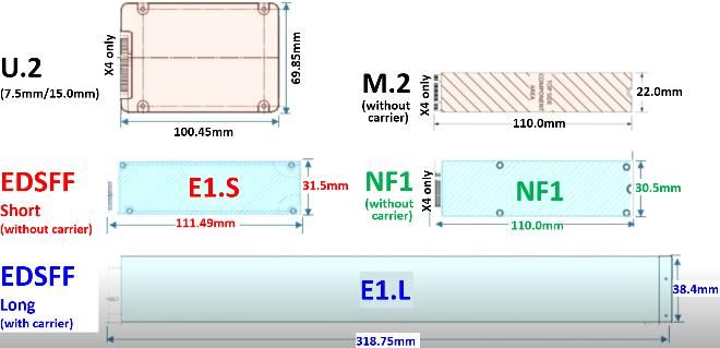
New SSD shapes allow for smaller and more powerful servers by packing more NAND die onto circuit boards for denser capacity. With improved power efficiency and thermal profile, they lower the effective cost per gigabyte and allow for new architectures. One radically disruptive shape is called Enterprise & Datacenter Storage Form Factors (EDSFF) or “ruler” for short. Storage rulers come in a short (EDSFF E1.S) and long size (EDSFF E1.L). Short rulers resemble M.2 drives and plug into the front of a server and support hot-swapping. Just 32 long rulers with dense QLC NAND give a server almost a petabyte of SSD storage in just one rack unit (1RU) as shown to the right.21 These designs are a clear change in data center removable storage versus the airflow and circuit board size limits of 2½" SATA, SAS, and U.2 drive form factors. The illustration on the right shows the height and width of these new ruler SSDs versus 2½” thin, 2½” regular SSDs, and large capacity 3½” hard drives. Some 1U servers accommodate a mix of rulers and U.2 drives by housing them in swappable independent sleds as shown to the left. Using 32 hot-swap U.2 NVMe drives in a removable deep modular enclosure and 16 hot-swap storage rulers in a removable modular enclosure, the server provides 1PB of storage space. In this scaled drawing, 24 U.2 SSDs (0.7PB) fit in 2U of rack space while 64 EDSFF rulers (~2PB or 2.6X denser) fits into the same space. If you compare the ruler to 12 x 4TB 3½” hard drives in 2U, the ruler is 46X denser. A full 42U rack of hard drives holds 903TB while a rack of rulers is about 41 petabytes, or conversely, the entire rack capacity of 3½” hard drives could be reduced to a single 1U of rulers. Compared to 2-millisecond latency for a 15K hard drive, any EDSFF can READ 3,200 MB/s and WRITE 1,600 MB/s in 135 microseconds.22 Dell.com/certification 7
Four additional form factors were designed by the EDSFF
Working Group. The EDSFF E3 comes in a long 3½” and a short
2½” drive depth in either a 7.5mm (about laptop drive size) or
16.8mm thickness.23 These 2U shapes will hold about 48 NAND
chips or roughly 50% more than a comparable U.2 drive.

Samsung’s NF1, originally called Next Generation Small Form Factor (NGSFF), is ⅓ wider and
longer than an M.2 2280 (22mm x 80mm) or about the
size of an M.2 30110. It’s larger circuit board holds 16
dies or 16TB of NAND.24 Sometimes referred to as an
M.3, it quadruples the M.2 capacity, provides hot-plug
front-bay serviceability, LED status lights, and uses SATA, SAS or PCIe interfaces.25 Its dual-
ported design adds high-availability for controller redundancy or dual-controller concurrent drive
access. The PM983 NF1 holds 15.36TB and is a fraction narrower than EDSFF allowing 36 of
them to provide a 1U server with 550TB of capacity.

This diagram depicts the relative size of the 4.4”
(111mm) E1.S, the 4.3” (110mm) NF1, and Intel’s
DC P4500 12½” (318mm) E1.L QLC ruler that fits
into a 1U server. The E1.S and NF1 have the
depth of a 2½” drive and six E1.S drives fit in the
space of two 2½” drives. With hard drives
becoming less popular, new form factors such as the ruler shape will allow for greater density.

New Interfaces
The twenty-year-old 8430 leverages SCSI hard drive technology from the mid-1980s. In 2003
SATA began replacing the Parallel Advanced Technology Attachment
(PATA) found in PCs of the day and soon evolved into an enterprise
standard. SATA supported “hot-swappable” replacement of failed drives,
provided fast I/O transfer rates, command queuing, and used small lower-
cost cables (shown to the right). 26 SCSI Ultra-3 was popular in 2000 and
had speeds of 160MB/s while supporting 15 drives per controller port. SATA eclipsed PATA and
SCSI with 187.5 MB/s (1.5Gb/s) per drive loop and reached 6Gb/s (750MB/s) by 2009.27 SATA
transfers data in half-duplex (one point-to-point link direction at a time). With SATA SSDs, half-
duplex became a processor bottleneck. There are no plans for a faster SATA interface.28

2020 Dell Technologies Proven Professional Knowledge Sharing 8
In 2004, SAS doubled the SATA bandwidth and maintained support for hard drives. Today, the
12Gb/s SAS-3 interface is still backward compatible with older SAS and SATA drives. SAS
allows 256 queued commands and supports up to 65,535 dual-ported drives. IDC predicts 70%
of enterprise hard and solid-state drives sold through 2022 will be SAS or SATA.29 Unlike half-
duplex SATA, full-duplex SAS allows data to be transmitted bi-directionally.

In 2003, PCIe was introduced as a high-speed motherboard slot interface that accepts a graphic
card, storage controllers, and other adapters. The latest version has
128GB/s (1,024Gb/s) of bandwidth. The open device NVMe is a key
efficient design element in a new SSD interface that also runs on
PCIe. NVMe improves application response time, increases bandwidth to dramatically boost
SSD performance, and reduces latency, which is the time a CPU wastes waiting for data. Just
as SATA and SAS SSDs replaced hard drives in mission-critical enterprise applications, NVMe
SSDs will make deep inroads into replacing legacy SSDs. Non-Volatile Memory devices attach
to the PCI Express bus and communicate directly with the CPU, so they do not need dedicated
storage bus controllers – hence the “NVMe” nomenclature.

In the past, making an application run faster often meant a processor upgrade. Moving storage
electrically closer to the CPU and simplifying the process stack
achieves the same goal through increased CPU utilization. This is
measured through lower latency, increased throughput, and faster
user response time. As this Linux storage stack illustration shows,
NVMe is much simpler than the hard disk-era SCSI stack used in the
SAS/SATA interface, allowing NVMe SSDs to be much faster than their counterparts.30

NVMe is not a physical connector so it
supports various form factors including a
traditional 2½” rectangular shape. U.2 NVMe
SSDs use the same connector but with
different pinouts - the PCIe in blue and the SAS and SATA in red. Internally, a PCIe NVMe
SSD can be an M.2, fit into a standard PCIe motherboard slot, or used as a “ruler.”

A double notch M.2 connector on the right side of this image indicates it is SATA and transfers
data at 6Gb/s while one notch means it is
PCIe NVMe and performs up to three
times the speed of its SATA counterpart.

Dell.com/certification 9
The current SATA and SAS architecture is almost a decade old. Conceived before SSDs came
to market and originally supporting hard drives, the combination of design and
throughput keeps them from delivering the full potential of today’s SSDs.
Processor performance doubles every two years and is impacted by relatively
slow I/O performance - the gap is increasing. SSDs made great inroads in
closing that gap, but it wasn’t enough.

One SSD can transfer 550-4,000 megabytes of data a second and a modern
interface allows them to work in parallel on a queued list of I/O commands.
With SATA-3’s maximum 550-600 MB/s transfer rate, a single SSD with
enough commands can be slowed by its interface. SAS-3 is twice the speed of SATA-3, and
while its story is better, it too runs into saturation issues that hamper performance. The
bottleneck gets worse when a bunch of SSDs on a single loop work on queued I/O commands.
When storage components perform suboptimally, the
CPU waits for I/O. There simply is not enough
bandwidth from their disk-era design to get the job
done. SATA-3 and SAS-3 SSDs are forced to
perform slower than 4,000MB/s NVMe devices even
though they generally employ the same NAND chips.

SSD nomenclature such as “PCIe 3.0 x 4” describes the older and popular PCIe version 3.0
interface with four serial point-to-point data transfer lanes. In One lane highway
 3 cars

this illustration, a PCIe lane is like a single versus a multi-lane Four lane highway
 12 cars
highway where all cars travel at the same speed. The only way
to increase highway throughput without speeding up the cars is
to add parallel lanes. Devices stripe data across multiple PCIe
lanes for increased throughput. A PCIe 3.0 x 4 device supports 4 x 985MB/s or 3.94GB/s in
each bus direction for a four-fold data transfer rate to and from an SSD. For more throughput at
the same speed, a PCIe 3.0 x 8 with eight 985MB/s lanes is used. Some NVMe SSDs transfer
4GB/s in a four-lane design while SAS is limited to 12Gb/s.31 Processors such as Intel’s i7-
8700K has 16 PCIe 3.0 total lanes while AMD’s EPYC has 128 PCIe 4.0 total lanes.32,33

NVMe is a vendor consortium design that permits SSDs to work in parallel # Queue
 Queues Depth
with low latency and support thousands of queued requests. It allows the SATA 1 32
 SAS 1 256
processor to run more virtual hosts and handle more database transactions, NVMe 65,535 65,536
thereby increasing core productivity and likely reducing core-based software licensing costs.34

2020 Dell Technologies Proven Professional Knowledge Sharing 10
NVMe supports 65,535 queues of 65,536 commands per queue, theoretically handling 4.3
billion commands compared to SAS and SATA’s single queue depth of 256 and 32
respectively.35

The SAS and SATA single queue approach worked fine for hard drives considering its head
movement rotational disk platter delays, but it became an issue when dozens or more SSDs
became common in large servers and storage arrays. The highway illustration depicts SAS and
SATA single lane local roads restricting the SSD to single queue activity.36 Today’s processors
with NVMe accomplish much more work than their predecessors.

SATA uses four non-cacheable CPU register READs per I/O command while NVMe doesn’t
need them.37 SCSI’s older storage stack is encumbered with a hard drive serial queuing I/O
approach that adds 2.5μs of latency when coupled with CPU overhead. A QLC PCIe NVMe
SSD (175,000 IOPs) random READ speed is 329 times faster than a SATA 7,200 RPM hard
 drive (532 IOPs), translating into more processing with less
 equipment.38 NVMe offers three times the IOPS of SAS SSDs
 SAS/SATA
 and twice the sequential READ throughput.39,40 A
 33% NVMe CPU overhead reduction Device Driver

 27,000 CPU Cycles
 compared to SAS or SATA complexity
 SCSI/SATA
from the PATA era allows the CPU to work on other tasks, NVMe Translation
 Block Driver
 CPU Cycles

 Device Driver
 10,000

use fewer cores, or consume less power. To the right are Block Driver OS Scheduling
 OS Scheduling & & CTX Switch
 CTX Switch
some of the SAS/SATA versus NVMe differences41: VFS 2000 vs 3000 VFS
 CPU Cycles

 • uses 27,000 CPU cycles to handle 1 million IOPS compared to 10,000 for NVMe
 • may need many controllers, each adding overhead
 • SCSI translation adds 3µs and 4,000 cycles while NVMe removes this step
 • consumes nearly 3x more CPU resources than NVMe
Just like an SSD helps improve system throughput compared to a hard drive, PCIe 3.0
improved the performance of the system bus that supported these SSDs and other adapters. In
2017, PCIe 4.0 doubled the performance allowing a server to support many more NVMe drives.

This year, PCIe 5.0-based servers will again double the total
bidirectional performance to 128GB/s. PCIe 5.0 quadruples
the legacy PCIe 3.0 standard, greatly improving virtualized
computing density.42,43 A single PCIe 5.0 lane at nearly 4GB/s
has almost 500 times the data throughput of the original PATA
PC interface. Work has begun on the PCIe 6.0 specification

Dell.com/certification 11
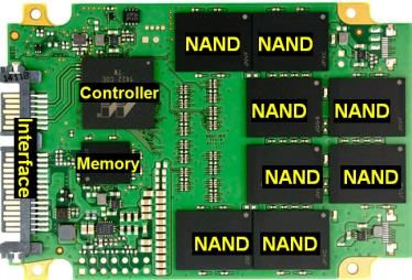
and in 2022 it should double performance yet again. These improvements allow NVMe devices
such as U.2, M.2, and the EDSFF rulers to remove a choke point and support more devices at
faster speeds. Lastly, NVMe drives cost about the same as SAS/SATA SSDs.

How Do SSDs Work?
At a high level, SSDs follow this generic image. Using a USB, SATA,
SAS or PCIe interface, they interact with a controller, memory/cache,
and one or more NAND chips on parallel channels. Some SSDs
physically combine functions like the controller and memory. And as
mentioned earlier, they come in different form factors.

The controller is critical to coordinating incoming host data requests, using memory to maintain
data placement tables, orchestrate READ/WRITE operations, perform garbage collection, and
map out bad cells. It also refreshes each cell’s charge to maintain data integrity thresholds since
they leak electrons. Without a charge, NAND cells can retain their contents for about 8 years at
room temperature or about a month in a very hot car.44
 Best Worst
The heart of an SSD is the NAND cell, and no one cell type is Performance SLC eMLC MLC TLC QLC

best for every workload. The NAND variants are: Endurance SLC eMLC MLC TLC QLC

 Price/GB QLC TLC MLC eMLC SLC
 1. Single-Level Cell (SLC) – Highest performing. Better
 WRITE endurance than eMLC. Used in enterprise-grade Density QLC TLC eMLC SLC
 MLC
 SSDs. Most expensive which hurts mass adoption.
 2. Enterprise Multi-Level Cell (eMLC) – Enterprise use. Higher write capability than MLC,
 but less than SLC. A lower-cost alternative to SLC.
 3. Multi-Level Cell (MLC) – Used to be mainstream. Slightly slower than SLC, it cost much
 less to produce. Lower endurance than SLC or eMLC.
 4. Triple-Level Cell (TLC) – Originally for budget-oriented SSDs. Has lower
 WRITE/reWRITE endurance than MLC and lower per-GB cost - a strong case for value.
 5. Quad-Level Cell (QLC) - Latest architecture with 33% more bit density than TLC NAND.

An SSD’s circuit board of NAND chips are
connected to channels that support multiple
independent parallel activities as directed by a
multicore controller. A NAND die is measured in
gigabits, and in this example each is 512Gb. We
have 4 die per channel and 8 channels for a 2TB SSD:45
 16,384
 4 8 ℎ 512 = = 2,048 = 2
 8

2020 Dell Technologies Proven Professional Knowledge Sharing 12
NAND die, controller and memory miniaturization reduce circuit board surface
area to keep costs low and improve performance. On the right, Samsung’s 1TB
QLC SSD needs just three chips for the entire device! The controller accesses 8
stacked QLC chips allowing it to process multiple requests in parallel.

Anatomy of a READ
Like a hard drive, a host sends a command such as a Windows READFILE to the SSD to find
specific data. The SSD controller gets the READFILE command and the address of the data
from the interface, and translates it into a request based upon the number of die, planes, blocks,
 and pages on the circuit board (see image to the left). SSDs can
 have 8 or more die with each having multiple planes. A plane has
 thousands of 256KB or 512KB blocks with 64 or more pages per
 block. A page has 32 rows of Host Page Lookup NAND Flash
 System Table Memory
 Sector Logical Physical Physical Block 1
 Address Page Page
32,768 cells representing 4,096 bytes (4KB). READs and 3 Address Address Page 1 1
 Page 2 2
 1 94
WRITEs are at the page level while erasure is on all 64 Page 64 64
 2 346 Physical Block 2
pages in the block (which explains why erasure takes a while.) On Page 1 65
 3 66 Page 2 66
the right, a Host issues a READ of NTFS Sector 3. The controller Page 64 128
 4 9
 Physical Block N
sends the contents of NAND Physical Block 2, Page 2 through N 813 Page 1 (N-1)*64+1
 Page 2 (N-1)*64+2
the SATA interface. The host is unaware the data was from an SSD. Page 64 (N-1)*64+64

SSD evolution makes the controller’s error correction capability
critical as NAND chips wear over time, suffer from weak bit
signal levels, experience electrical “noise”, or have “stuck” bits.
Error Correcting Code (ECC) ensures data written to NAND
chips are reliably READ back without error. When ECC
struggles to correct errors, the cell is deemed unreliable and a
fresh cell takes its place. In this example, the value 11011111
is written to the SSD along with extra error parity bits in yellow. With a host READ request, an
algorithm employs parity correction bits to determine the data stored 11001111 has an error as
shown by the red bit, and corrects it back to the original string 11011111.

Unlike hard drive fragmentation, SSD fragmentation occurs as data is deleted or rewritten such
as when the Windows recycle bin is emptied (TRIM command) or Word “Saves” a document.
NAND chips cannot rewrite in place so discarded data is erased when revised, good data is
moved to a new page and the block is erased. Defragmentation housekeeping uses background
garbage collection when the SSD is idle or ASAP if space is needed for write activity. Assume

Dell.com/certification 13
Block A Block A Block B
Block A has 6 pages. Page data4 needs updating and old data needs data1 free data1
 data2 free data2
erasing. All data pages are copied to new Block B and Block A is old data free data3
 data3 free update data4
erased to a “free” state. Writing a free block is faster than rewriting data. old data
 data4
 free
 free
 free
 free

A controller experiences write amplification (WA) overhead when it writes more blocks to free up
space than the host request. For example, writing 512 bytes to a 4KB page is a WA of 8
 4
(512 = 8). Excessive writing prematurely wears out an SSD, so it is stored in a buffer until

there is a sufficient amount to optimally write out. Garbage collection adds to write amplification.

Intelligent arrays tackle WA issues through caching algorithms. “Write folding” replaces similar
WRITEs in memory and puts the final one on NAND such as when a program rapidly updates a
counter.46 “Write coalescing” groups small WRITEs into a large one for better page alignment.

What is a Cell?
The NAND cell is the heart of an SSD. A cell is a transistor-inspired device called a Floating
Gate Metal-Oxide-Semiconductor field-effect transistor or FGMOS.
An oxide insulation layer makes it non-volatile as it traps electrons in
the floating gate. The lack or presence of floating gate electrons
represents the binary values 0 and 1. Operations use the gate, source, and drain terminals.

To read from a cell, the controller sends a test voltage to the control gate at the cell’s address.
With SLC, if the floating gate has an electron charge, that number of electrons is prevented
from flowing between the source and drain for
a binary 0 as shown to the left. Without a
charge, all electrons flow between the source
and drain for a 1 as shown on the right.

To WRITE or program the floating gate, a high voltage of about +20
volts is put on the control gate. A quantum physics Fowler-Nordheim
Tunneling (FNT) process causes electrons to flow from the source and
drain through the semiconductor and oxide barrier and land in the
floating gate. An SLC floating gate is a logical 0 with electrons and 1 without electrons.

ERASING is FNT in reverse. When the control gate receives -20 volts,
any built-up floating gate charge escapes through the oxide layer and out
the source and drain, resetting the FGMOS to no charge or 1.

2020 Dell Technologies Proven Professional Knowledge Sharing 14
Enter Quadruple-Level Cell SSDs
The mapping interpretation of floating gate voltages to logical bits per cell sets the different
types of NAND cells apart. In 2006, SSDs used an SLC floating gate that either had a charge or
it didn’t. In 2009, an MLC stored 2 bits in the floating gate with 3 bit TLC following 7 years later.
Each enhancement lowered NAND cost by increasing gigabyte wafer yields which helped drop
SSD prices. SLC improvements by-and-large made single-layer silicon planar circuits smaller
while today’s improvements are focused on increased capacity through multi-cell technologies
and three-dimensional multilayer circuits.

A QLC FGMOS drain has 16 voltage levels between 0.0 and 1.0 corresponding
to values 0000 through 1111 as shown to the right. The same FGMOS is used
in an SLC, MLC, TLC or QLC cell, differing only in the binary interpretation of
the drain voltage. An SLC drain either has a voltage (programmed) or it doesn’t
(not programmed) corresponding to a binary 0 or 1. A 2 bit MLC at .33 volts
represents 01 while the same .33 volts is 0101 in a 4 bit QLC. Storing more bits
increases the READ, WRITE or ERASE times.

 SSDs boost the performance of mission-critical, I/O starved
 applications. Two years ago, QLC SSDs incrementally advanced
 enterprise storage.47 SATA QLCs are one-for-one plug-compatible
 replacements for hard drives since they are quiet, use less power,
 and are faster with a 7-10X latency reduction as shown to the left.

A single SATA QLC SSD, which might use SLC NAND for caching, often replaces many rotating
high latency 10K and 7,200 RPM low IOP hard drives just as TLC SSDs replaced 15K hard
drives. From an IOP perspective, using QLC SSDs can translate into a reduction of data center
racks.48 QLC has 175 times faster random READ and 30 times faster WRITE performance than
hard drives, and use less power and cooling. The popularity and advantages of QLC may force
the hard drive market into niche use cases of cold data storage applications as these SSDs
become more reliable and affordable.

While many applications do more reading than writing, the downside to QLC is its limited daily
write duty cycles, making them suited to READ-intensive environments.49 To evaluate your
environment, review the procedure in the paper “Understanding Windows Storage IO Access in
the Age of SSDs”.50 Micron’s 5210 QLC SSD is rated for 0.8 drive writes per day or 6.4TB/day
of writing on an 8TB drive - a hefty amount. This topic will be covered in detail later in this paper.

Dell.com/certification 15
Workload I/O patterns tend to follow application profiles. QLC SSDs are a good fit for modern
applications where data is written or rewritten infrequently
and read often such as content delivery (e.g. Netflix), video
streaming and other limited-changing data.51 Write-intensive
and data backups, database logs, and ingestion workloads
should be on SLC - TLC. While machine learning algorithms
feeding artificial intelligence may have 5,000 READs per WRITE, On-Line Transaction
Processing (OLTP) is WRITE- and READ-intensive and best suited for MLC or TLC.52

SSD profiles are analyzed with Self-Monitoring, Analysis and Reporting Technology
(S.M.A.R.T.) or Windows PerfMon. Micron found a particular server spent 99% of its I/O doing
READs – a perfect candidate for QLC SSDs.

Quad-Level Cells look like an easy concept, but are they?
As discussed, FNT is key to floating gate electron retention and erasure. However, the high
voltage needed to WRITE or ERASE a cell also destroys the oxide layer’s insulating properties
little-by-little every time it is performed. Voltages used to READ are low and do not damage the
tunneling oxide, but writing and erasing gradually wears out a cell, making voltages inexact.

Cell types to the right have different program/erase (P/E) cycles (also called SLC Endurance 100,000
 P/E Cycle
 eMLC 35,000
wear cycles or write cycles.) Some are more resilient than others and
 MLC 10,000
given values are not absolute. Enhanced wear leveling, bad-block eTLC 10,000

remapping/overprovisioning, error correction and write algorithms TLC 3,000
 QLC 1,000
increase an SSD’s life. The SSD controller recovers marginal cell
data and restores it to viable cells. An SSD incapable of write activity still provides the data in
“read-only” mode. SSDs can take years to wear out and usually become obsolete before
reaching P/E limits. SLC cells can be written 100,000 times while QLC only 1,000 times. Higher
cost enterprise NAND prefaced by “e” have higher P/E ratings because of more efficient
controller design, giving eMLC a 35,000 P/E rating or three times the MLC value.53

As cells wear, their drain voltages fluctuate and it is hard to
determine their binary value. In this QLC diagram, a controller
sends the host 0111 when it reads .47 volts from a new cell or
between .44 and .49 as the oxide wears down. The host
receives 1000 for .50 - .56 volts and 1001 for .57 - .62 volts.

2020 Dell Technologies Proven Professional Knowledge Sharing 16
QLC depends on its controller’s ECC to ensure stored values are read correctly. If a READ fails,
its’ block is labeled an unreliable “bad block” and swapped for an "overprovisioned” reserve one.
A drive nearing failure has increased ECC overhead causing higher response time. An SSD can
have 25% or more reserve blocks based on its warranty.

Producing QLC chips is difficult. NAND dies are cut from large etched silicon 1 2 3 4 5
wafers and a percentage of them fail during testing. Rectangular dies also 6 7 1 2 3 8 9
 10 4 5 6 7 8 11
don’t fit well on circular wafers as shown here - 21 fit while 24 are 12 9 10 11 12 13 13
incomplete. Yield equals the number of viable dies after discarding failed 14 14 15 16 17 18 15
 16 17 19 20 21 18 19
or incomplete ones. A 300mm wafer yields 148 20mm dies.54 Currently,
 20 21 22 23 24
the 64-layer TLC’s reliable die yield is at 90% while QLC is 48%, meaning only half of the QLC
dies can be used in an SSD.55 High yield levels are necessary for significant price reductions.

Later this year, Intel and Toshiba plan to introduce 5-bit Penta-Level Cell (PLC) NAND. PLC is
expected to support half the write cycles of QLC with a price profile making it compelling to
WRITE-once, READ-many applications.56

The Big Paradigm Shift – Multi-Level NAND Cells
For years, the semiconductor industry followed pioneer Gordon Moore’s 1965 prediction that
transistor density would double every 24 months. NAND density increased while circuit paths
decreased, resulting in lower gigabyte costs. Improvements in photolithography allowed even
tinier NAND die. Eventually, makers increased density and lowered costs by building circuits
higher rather than increasing surface area – another of Moore’s predictions.

As shown to the right, the storage industry reduced high development costs
 TSV
by moving from Two Dimensional (2D) Planar NAND to Three
Dimensional (3D) NAND. Packing the maximum number of chip
 components into the minimum
 volume is analogous to a high-
 rise building or skyscraper shape 2D Planar NAND 3D NAND
 with underground tenant parking instead of 1-2 story houses. 3D
 NAND stacks multiple layers interconnected by tiny channels called
 Through Silicon Vias (TSV). Processing logic is kept in the base
 and is used to communicate to all NAND layers within the die, all
while keeping the same footprint area.

Dell.com/certification 17
All NAND uses transistors, but some manufacturers reorient
3D NAND using charge trap flash (CTF) to lower lithography
costs and TSV scaling complexities.57 In a departure from
planar NAND, Samsung’s V-NAND boosts cell endurance,
minimizes the footprint, and keeps electrons in a non-
conductive silicon nitride (Si3N4) insulating layer rather than in a floating gate conductor. The
control gate is wrapped around the CTF. “Discs” are stacked and the address bitline connects
each charge trap cell. The CTF’s thin insulator uses a lower erase voltage, so cells last longer
than classic floating gate cells.58 The READ/WRITE/ERASE rules are similar.

CTF vertical alignment triples the inter-cell gap reducing the data corruption found in dense
planar NAND. Stacked column cells are twice as fast,
denser, more energy-efficient, and cheaper to produce
than 2D designs.59 Bitlines run in the block’s “Z” axis and
span the chip’s layers. The insulator covers the bitline
and the wordline connects each layer’s control gates.60

The 1 to 4-bit cell progression and the advent of 64+ layers make storage denser, cheaper per
bit, and faster than planar NAND. NAND gigabyte pricing should dip below 10¢ this year or 3X
the cost per hard drive gigabyte.61 Layer counts should reach 256
this year and 512 by 2022 – an 8X increase over 64-layers.62
Extrapolation shows today’s 16TB U.2 SSD will be dwarfed by a
128TB unit in just three years, accelerating the per-gigabyte price
decrease. A 1U rack of 32 x 170TB dense rulers should exceed
200PB this year. Contrast that with our 5.4PB 8430 example and we see everything changing.

Endurance Is a Big Question
Hard drive endurance issues stem from their mechanics. A study of
25,000 hard drives showed that nearly one in five fails within four
years, and within 6 years, half have failed.63 Data loss is mitigated
through parity, backups, snapshots, data center disaster recovery
planning, and other methods.

When SSDs were new to enterprise solutions, storage architects did not have a good feel for I/O
profiles and feared WRITE endurance was the device’s “Achilles heel”. Conservative designs
called for drives that could tolerate dozens of Drive Writes Per Day (DWPD). DWPD is the

2020 Dell Technologies Proven Professional Knowledge Sharing 18
number of times all SSD data could be rewritten daily and remain in warranty. It usually refers to
“sequential” large block versus “random write” small block I/O because of the increased wear
caused by write amplification.

To look at the wear on your Windows 10 SSD, use this PowerShell command:
 PS C:\> Get-PhysicalDisk | Get-StorageReliabilityCounter | Select Wear
The answer returned is a wear percentage. On my PC, I get 6%: Wear
 6
As a rule of thumb, a 0.1 DWPD indicates a “READ-intensive” SSD and a higher value such as
10 would be “write-intensive.”64 TeraBytesWritten (TBW) can also help evaluate different SSDs
since its numerical value is not tied to the SSD size or warranty. For example, the statement “1
DWPD” for a 1TB SSD means something completely different for an 8TB SSD.

Over time, real-world workload experience allowed for
more accurate predictions and selection of optimal SSD
technology. This application characterization chart shows
the willingness of architects to deploy the right cost-
effective technology. In 2006, SLC SSDs with 10 DWPD
were popular, but by 2016, 61% of SSDs shipped could
handle up to 1 DWPD (a threshold for QLC) and 89%
supported up to 5 DWPD.65 This year, 90% are less than 1 DWPD and 99% up to 5 DWPD. It is
projected that fewer than 1% of applications will need >10 DWPD by 2022, demonstrating a
shift to READ-intensive SSD technology. It is hard to imagine today’s 100TB data lake being
built with slow hard drives over modern 3- and 4-bit SSDs based on cost, performance, and
reliability.

Let’s explore the meaning of an SSD wearing out by reviewing its warranty. Samsung’s 480GB
2½” SATA-3 SSD SM883 has a DWPD of 3.0 and a 5-year warranty – a useful life of:
 480GB x 3 DWPD x 365 days a year x 5-year warranty = 2,628,000GB.
Over 2.6PB can be written to this drive under warranty – Month GB/day Total GB GB remain
a lot of data! Assume you need to write 500GB a day to 1 500 2,628,000 2,613,000
 2 500 2,613,000 2,598,000
this drive for 60 months, this table shows there’s a lot of
 3 500 2,598,000 2,583,000
useful drive life left and it would likely last you an
 ⋮ ⋮ ⋮ ⋮
additional 60 months. 60 500 1,743,000 1,728,000

TLC and QLC have the same sequential READ speed, so the key to selecting the right SSD
model for your application or system is to know the average number of bytes written in a day.

Dell.com/certification 19
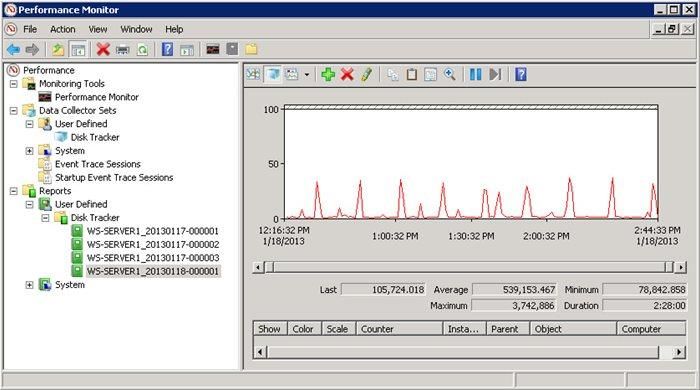
Begin an analysis by collecting data on the Performance Monitor

most active day using Window’s PerfMon or
the Linux’s sar or iostat command to report
on the average number of bytes written per
second.66 Extrapolate it out for one day – a
system that writes 539,153 bytes per
second (540,000 rounded) x 60 seconds
per minute x 60 minutes per hour x 24
 Average 539,153.457
hours per day, or
 540,000 x 60 x 60 x 24 = 46,656,000,000 bytes of data written per day.
Convert that to gigabytes and you get 43GB/day. On an annual basis,
 43.45GB x 365 = 15,859GB/year or 15.49TB/year.
If the drive has a 5-year warranty,
 15.49 x 5 years = 77.45TB/drive warranty period.
A 77TB warranty is sufficient. Anything less and you are buying the wrong SSD. The paper cited
earlier, “Understanding Windows Storage IO Access in the Age of SSDs”, has additional
examples.67 If you are using a Redundant Array of Independent Disks (RAID) to protect against
drive failures, you are further protected against data loss. Intel and others often add SLC cache
to QLC SSDs to increase the device’s useful DWPD warranty life and also boost performance.68

As a general rule-of-thumb69:
 Use Case Approx. SSD DPWD
 Boot Drive 0.1 ~ 1.0 random
 Content Distribution 0.5 ~ 2.0 sequential
 Virtualization and Containers 1.0 ~ 3.0 random
 OLTP Database ~ 3.0 random
 High Performance/Caching ~ 3.0 random

Understanding QLC Data Profiles - What Workloads Work Best?
The 8430 or DMX-4 had many 10K RPM hard drives that reflected a compromise between very
expensive and small 15K RPM and even slower but cheaper and larger 7.2K RPM drives.
Businesses opted to make this concession because they were budget-constrained and many
applications did not need 15K RPM drives. As a result, data workload classification employed
tiers of fast and slow hard drives in different RAID types. Administrators faced with solving ultra-
fast low-latency business problems may have even used “short-stroke” hard drives.

2020 Dell Technologies Proven Professional Knowledge Sharing 20
A few years ago, voluminous read-only data was relegated to large 8-14TB hard drives or even
magnetic tape. As capacity requirements grew and new storage projects arose, the need for
lower cost, greater reliability and speed improvement found organizations replacing hard drives
with QLC SSDs. A server such as Dell’s R720xd 1 2 3 4 5 6 7 8 9 10 11 12 13 14 15 16 17 18 19 20 21 22 23 24

with 24 x 2½” front-drive slots might use 2TB 7.2K
SATA hard drives. They could be replaced by just 8 x 2½” 8TB QLC SATA SSDs for 64TB of
capacity (38% more) and 720,000 4K random READ 1 2 3 4 5 6 7 8 9 10 11 12 13 14 15 16 17 18 19 20 21 22 23 24

IOPS (375 times more), saving on power and
cooling, and providing 16 open slots for future expansion.70 With a full set of 24 QLC drives, it
could deliver two million IOPS and 768TB of capacity with 4:1 compression techniques and
provide a fast storage platform for analytics, CEPH, NoSQL, and big data applications.

Trend lines show that customers who still buy hard drives
are part of a shrinking minority. Just like vacuum tubes
gave way to transistors, the world is surely heading to
SSDs. Hybrid systems of hard drives and SSDs made
great sense when SSDs had a small capacity and were
 expensive, but now their sizes rival and exceed hard drives while
 Block

 >100ms

 their cost profile had been steadily decreasing and now hovers at
File Type
 File

 just over twice the price.71 That does not mean hard drives will
 become extinct since there will continue to be use cases for
 Object

 inexpensive spinning media.

Intel Optane
From an endurance perspective, QLC NAND is a good fit for READ-intensive environments. But
what would you choose if you needed WRITE-intensive ultimate performance storage? A few
years ago, an SLC NAND would be a good solution, but now there is a superior technology.

Optane is Intel’s brand name for 3D XPoint (pronounced “cross
point”) transistor-less technology co-engineered with Micron. It is a
low-latency non-volatile memory that is faster than NAND and
supports near-infinite WRITE endurance. Fear of prematurely
wearing it out is unwarranted since the U.2 DC D4800X is rated for
60 DWPD versus 3 DWPD for a NAND SSD.72

Dell.com/certification 21
3D XPoint uniquely stores binary values making it an excellent choice for WRITE-intensive
database redo logs or caching.73 It is 4X–10X faster than NAND, consumes less power and
permits a cell to be both addressed individually and overwritten/updated removing the need for
garbage collection. Micron’s QuantX implementation is rated for 2.5M IOPS, supports 9GB/s of
READ/WRITE bandwidth, and has latency under 8μs compared to 95μs MLC NAND.74,75 It
doesn’t need a reserve capacity and may only need a limited ECC.

Unlike NAND, Optane does not have a control gate,
oxide barrier or use FNT to move electrons. When a
voltage is applied to a selector’s top and bottom
wire, one cell is read or written in contrast to a
NAND’s page at a time approach. Using a Phase
Change Memory (PCM) such as chalcogenide glass,
the state of the glass is altered from amorphous (clear or 0) to crystalline (opaque or 1) like a re-
writeable recordable DVD.76,77 It is dense when stacked in a grid of 128 billion cells per die.78,79

Storage evolution trends are clear and the revenues
generated by these products are undeniable. This
IDC chart shows PCIe storage will reach over 60%
market share this year as older SSD technologies
age out.80

What’s new in storage?
NVMe and Just a Bunch of Flash
As discussed, NVMe slashes latency, supercharges parallelism and
significantly improves SSD throughput beyond the hard drive architecture.
Rather than attach and funnel data through a SAS/SATA controller, NVMe
SSDs connect at PCIe speed to the CPU. One such NVMe SSD design
outside the server is “Just a Bunch of Flash” or JBOF. JBOFs do not use
RAID controllers but present NVMe SSDs to a processor over a PCIe bus. Servers run software
to manage SSDs as if they were direct attached.

JBOF is neither a SAN nor an HCI since it doesn’t share resources, lacks thin provisioning,
hardware RAID protection, high-availability, and other typical storage array functionality. JBOF
is for ultra-high performance, low latency use cases where there are more devices than server

2020 Dell Technologies Proven Professional Knowledge Sharing 22
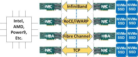
slots, such as with a blade server. SuperMicro’s JBOF uses 32

 NVMe 2.5” x4

 NVMe 2.5” x4

 NVMe 2.5” x4

 NVMe 2.5” x4
 12 NVMe 12 NVMe
 2.5” x4 2.5” x4
EDSFF E1.L rulers through 64 PCIe lanes to share 64GB/s of
throughput among 8 different servers.81 As shown, ZSTOR’s 24 Backplane
 PCIe Switch PCIe Switch
NVMe SSD’s on 4 lanes can assign groups of up to 12 drives to
 8 x PCIe 3.0 x 4 ports 8 x PCIe 3.0 x 4 ports
8 hosts through PCIe switches.82 Rear Panel - ZSTOR NV24P JBOF

 For decades, the Direct Attached Storage (DAS) model shown to the left incorporated
 drives in the server’s chassis for optimal performance and simplicity.83 While easy, one
 server might have excess unused capacity and another might be out of space. On the
 right, server #1 has two unused SSDs, server #2 has one
unused SSD and server #3 uses all three. If server #3 needs a fourth
drive, it has no open slots. For this and other reasons such as ease of
management, classic SANs came to be.

 By placing SSDs into a JBOF, drives are allocated as needed as
 shown to the left. In this case, it is easy to assign a single drive to
 server #1, two to server #2, and four to server #3. With room for
 future growth, no waste and no inter-server Ethernet latency, JBOFs
 are a low-cost approach to creating a Software-Defined Storage
 SAN.

As shown to the right, JBOF designs can also be scaled beyond a one-to-one host
and target relationship using an ultra-low latency PCIe switch. Multiple switches
can also help create a highly available JBOF storage system.

NVMe Over Fabrics
With designs such as HCI, applications may run slower if the CPU is taxed when sending large
amounts of data to storage. It happens when the inter-server transmission uses a high overhead
protocol such as TCP/IP across a small bandwidth network. Some companies addressed this by
adding servers and distributing the workload accordingly. Newer HCI designs use NVMe over
Fabrics (NVMeF) - an ultra-low latency, high throughput solution that frees the CPU of a lot of
overhead and allows SSDs to be on a network outside of a server’s PCIe bus similar to JBOF.

NVMe was designed to use a reduced latency Remote Direct Memory Access (RDMA) protocol
allowing a storage device to receive data from main memory without cache, CPU, or operating
system involvement. RDMA allows two servers to share data in their memory without using CPU
cycles, allowing the processor to focus on application processing. In its simplest form, there is a

Dell.com/certification 23
pointer to data to be moved, a pointer to where it should go, and a quantity. The CPU bypasses
TCP/IP and doesn’t use I/O cycles on SATA or SAS host adapters - the essential difference
between NVMe and SCSI.84 RDMA copies
data to or from an SSD to the processor’s
memory over a network using RDMA-ready
adapters as shown here.85

NVMeF leverages RDMA over an existing Fibre Channel (FC), Ethernet, Internet Wide-Area
RDMA Protocol (iWARP), or InfiniBand network. With Ethernet, RDMA employs Converged
Ethernet or RDMA over Converged Ethernet (RoCE
pronounced “Rocky”). Converged Ethernet uses RDMA
on the same Ethernet switches and cables a customer
already owns and TCP uses existing NIC cards.

NVMeF achieves the performance of direct-attached SSDs while sharing a standard SCSI
network. The difference between local and NVMeF-attached storage was minimized and adds
less than 3% or
A storage device rarely approaches theoretical performance levels on a day-to-day basis. A ten-
year-old SAN could support many simultaneous 100-200MB/s hard drive transfers but ran into
bottlenecks with a similar number of 550-1,100MB/s SSDs. A single 3,500MB/s NVMe SSD’s
theoretical throughput is throttled by 75% on
an 8Gb/s FC, 50% on a 16Gb/s FC link, and
could nearly saturate a single 32Gb/s FC link.
This chart plots hard drives, SSDs, EDSFF
rulers and Optane drives against transfer
rates.88 It shows the limitation of 10, 40 and
100Gb Ethernet and 16Gb/s and 32Gb/s FC
as full throughput is reached by a handful of
high performing drives. A single SATA SSD runs fine on a 10Gb/s network while a bunch of
them could saturate it. The same is true for NVMe SSDs. Just one NVMe drive likely runs fine
on a 25-gigabit link but with a bunch of very active drives, their high performance will be slowed
by that link speed. Individual 100GbE ports will bottleneck four NVMe TLC SSDs at theoretical
transfer rates. The optimal networking solution for NVMe is a 400GbE switch.

Modern motherboards and processors using four PCIe 3.0 bidirectional lanes can provide
3.9GB/s (3,900 gigabits) of bandwidth, or about the capability of one NVMe SSD. Just 6 NVMe
drives running at full capacity makes PCIe a new bottleneck and would limit the number of
active Ethernet or other devices that share these Bandwidth Bandwidth Bandwidth Bandwidth Bandwidth
 Year PCIe GB/s 1x GB/s 2x GB/s 4x GB/s 8x GB/s 16x
lanes.89 In other words, a server reading a lot of 2010 3 0.98 1.97 3.94 7.88 15.80
 2017 4 1.97 3.94 7.88 15.75 31.50
NVMe data could lack the resources to transmit 2020 5 3.94 7.88 15.75 31.51 63.00

those results anywhere else. It is worth noting that EDSFF drives are PCIe 4.0 and 5.0 ready.

PCIe 4 doubles the bandwidth to 7.88GB/s allowing SSDs to use fewer lanes. As a result, a
system could support more drives or have active SSDs get more parallel work done.90 PCIe 5
again doubles the bandwidth to 15.75GB/s. This line
thickness diagram shows the amount of I/O traversing
the CPU and RDMA adapter at each PCIe revision.

A single 32-ruler PCIe 4.0 4K movie content delivery server lacks the bandwidth and processor
power to simultaneously stream 64,000 movies (102GB/s or 3,200MB/s x 32) since it also needs
multiple 100Gb/s Ethernet NICs that also consume PCIe resources. With 8K movies, 4X more
bandwidth is needed and mapping one Ethernet or FC link to one NVMe QLC SSD for movie
streaming becomes impractical.91

Dell.com/certification 25
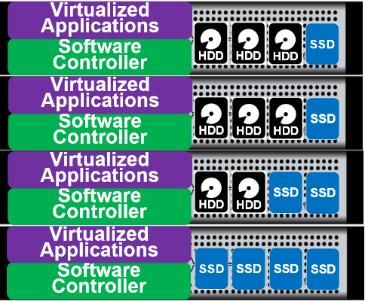
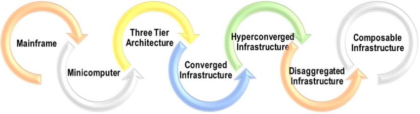
The good news is that for the most part, SSDs do not run at theoretical maximums and when
NVMeF was benchmarked against SCSI over 32Gb/s FC, it provided 58% more IOPS with 11-
34% lower latency.92 Testing showed NVMeF added just 10µs of latency compared to 100µs for
SCSI FC.93 The Fibre Channel Industry Association also has plans for 128Gb/s and the
Ethernet roadmap calls for faster 200Gb/s speeds.94,95

Software-Defined Storage
Three-tier SANs have been a staple of data center architecture for
twenty years as storage demand grew faster than server drive slots.
DAS issues of unused capacity were addressed through Ethernet
and FC networks that provided storage pooling, LUN assignment,
independent vendor choice for each tier, and more. In a storage
array, the software runs on a processor that handles incoming host
I/O requests and other management functions. Those requests may
flow through switches to aid resource sharing.

SDS is viewed as a lower cost SAN without vendor hardware lock-in, offering substantial OpEx
and CapEx savings, reducing storage provision time, and simplified
 Software-Defined Storage
management compared to a SAN.96 SDS is a loose definition that
abstracts traditional hardware-based storage services to manage internal or external virtualized
storage resources. It was designed to automate daily configuration, tuning tasks, and abstract
storage services, making it possible to have a Software-Defined Storage network made up of
multi-vendor commodity servers from Dell Technologies, HPE, Lenovo, and others.

Converged Infrastructure (CI) and HCI began over a decade ago as an easy way for companies
to consume prepackaged software, servers, networking, and storage
SAN components. HCI shrunk the SAN design into an all-in-one set
of clustered server nodes that pool virtualized compute and storage
resources. Both approaches allocate storage from internal disks on
demand through software to local server applications or non-
participating servers as though they came from a storage array such as a Dell EMC Unity.

As application virtualization became popular, CI and HCI using SSDs and cloud computing
brought about further design changes. Increases in storage speed and density, ease of
administration, provisioning, compression/deduplication, replication, snapshots, and other
enhancements also helped change storage architectures. Storage virtualization became popular

2020 Dell Technologies Proven Professional Knowledge Sharing 26
You can also read