Electronic transport in atomically precise graphene nanoribbons
←
→
Page content transcription
If your browser does not render page correctly, please read the page content below

Electronic transport in atomically precise graphene
 nanoribbons

 Juan Llinas

 Electrical Engineering and Computer Sciences
 University of California at Berkeley

 Technical Report No. UCB/EECS-2020-131
 http://www2.eecs.berkeley.edu/Pubs/TechRpts/2020/EECS-2020-131.html

 June 1, 2020
Copyright © 2020, by the author(s).
 All rights reserved.

Permission to make digital or hard copies of all or part of this work for
personal or classroom use is granted without fee provided that copies are
not made or distributed for profit or commercial advantage and that copies
bear this notice and the full citation on the first page. To copy otherwise, to
republish, to post on servers or to redistribute to lists, requires prior specific
permission.
Electronic transport in atomically precise graphene nanoribbons

 By

 Juan Pablo Llinas

 A dissertation submitted in partial satisfaction of the

 requirements for the degree of

 Doctor of Philosophy

 in

 Engineering- Electrical Engineering and Computer Sciences

 in the

 Graduate Division

 of the

 University of California, Berkeley

 Committee in charge:

 Professor Jeffrey Bokor, Chair
 Professor Ali Javey
 Professor Michael Crommie

 Spring 2020
Electronic transport in atomically precise graphene nanoribbons

 © Copyright 2020
 Juan Pablo Llinas
 All rights reserved
Abstract

 Electronic transport in atomically precise graphene nanoribbons

 by

 Juan Pablo Llinas

 Doctor of Philosophy in Electrical Engineering and Computer Sciences

 University of California, Berkeley

 Professor Jeffrey Bokor, Chair

 Advancements in on-surface materials synthesis have led to the development of
atomically precise graphene nanoribbons (GNRs). Bottom-up synthesized GNRs have
promising electronic properties for high performance field effect transistors (FETs) and
ultra-low power devices such as tunneling FETs. However, the short length, wide band gap,
and random orientation of GNRs have impeded the fabrication of devices with the expected
performance and switching behavior. In this dissertation, progress towards integration of
bottom-up synthesized GNRs into electronic devices is presented. The understanding of
GNR growth and band structure is surveyed and analyzed with a focus on the implications
on device yield and performance. The development of a device fabrication strategy for on-
surface synthesized materials is shown, with a focus on the fabrication of high on-current
and high on-off ratio 9-atom wide GNR FETs. Furthermore, device fabrication is
developed for FETs with parallel arrays of GNRs transferred from single crystal Au(788),
which greatly improves device yield. Finally, theoretical charge transport in GNR
heterostructures is employed to demonstrate exotic device behavior such as ultra-sharp
switching and negative differential resistance. The path towards state-of-the-art GNR-
based logic circuits is charted in this work.

 1
This work is dedicated to my mother, Nilsa Mesa.

 i
Contents
1 Introduction ............................................................................................................................ 1
 1.1 Electronic structure of graphene, carbon nanotubes, and graphene nanoribbons .... 1
 1.2 Field-effect transistors with 1-dimensional semiconductors ........................................ 3
 1.3 Dissertation organization .................................................................................................. 4
 1.4 References ............................................................................................................................ 4
2 Bottom-up chemical synthesis of graphene nanoribbons ................................................. 6
 2.1 GNR precursor.................................................................................................................... 8
 2.2 Growth surface.................................................................................................................. 10
 2.3 Polymerization dynamics and improving length distribution ................................... 11
 2.4 Solution synthesis ............................................................................................................. 13
 2.5 Growth of GNR heterostructures ................................................................................... 14
 2.6 Conclusions ....................................................................................................................... 15
 2.7 References .......................................................................................................................... 16
3 GNR transfer and device fabrication ................................................................................. 18
 3.1 Optical lithography of the device substrate ................................................................... 18
 3.2 GNR transfer ..................................................................................................................... 20
 3.3 Electron beam lithography .............................................................................................. 21
 3.4 Conclusion ........................................................................................................................ 22
 3.5 References .......................................................................................................................... 22
4 Band gap of graphene nanoribbons ................................................................................... 24
 4.1 Scanning Tunneling Spectroscopy ................................................................................. 24
 4.2 First principles calculations............................................................................................. 25
 4.3 Photoluminescence-emission spectroscopy of solution GNRs .................................. 27
 4.4 Resonant Raman spectroscopy of 7AGNRs .................................................................. 29
 4.5 Conclusion ........................................................................................................................ 32
 4.6 References .......................................................................................................................... 32
5 Field effect transistors with atomically precise armchair graphene nanoribbons........ 34
 5.1 Fabrication of FETs with 50 nm back gates .................................................................. 35

 i
5.2 9AGNRFET and 13AGNRFET characteristics and contact analysis ......................... 37
 5.3 Improving transmission across Schottky barrier via efficient electrostatic gating .. 40
 5.4 Device yield and variability ............................................................................................. 41
 5.5 Conclusion ........................................................................................................................ 43
 5.6 References .......................................................................................................................... 43
6 Field effect-transistors with dense, aligned graphene nanoribbons............................... 46
 6.1 Aligned GNR transfer and device fabrication............................................................... 46
 6.2 Transfer characteristics of FETs with parallel arrays of 7AGNRs .............................. 48
 6.3 Transfer characteristics of 9AGNR and 5AGNRFETs ................................................ 49
 6.4 Device yield and variability modeling............................................................................ 51
 6.5 Conclusion ........................................................................................................................ 53
 6.6 References .......................................................................................................................... 54
7 Towards high performance FETs: narrow band gap graphene nanoribbons ............... 55
 7.1 Band gap engineering using topological protected states in GNRs ........................... 55
 7.2 Field-effect transistors with a TE-GNR ......................................................................... 57
 7.3 TE-GNR FETs ................................................................................................................... 58
 7.4 Conclusion ........................................................................................................................ 60
 7.5 References .......................................................................................................................... 60
8 Super-lattice graphene nanoribbon field effect transistors ............................................. 62
 8.1 Band structure of SL-GNRs............................................................................................. 63
 8.2 Atomistic calculations of a SL-GNR FET ...................................................................... 64
 8.3 Analytical transport model using Landauer formalism .............................................. 66
 8.4 Bistable inverter with SL-GNR FETs ............................................................................. 72
 8.5 Requirements for experimental demonstration of SL-GNR FETs ............................. 73
 8.6 Conclusion ........................................................................................................................ 73
 8.7 References .......................................................................................................................... 74
9 Conclusion ............................................................................................................................ 75

 ii
Table of figures
Figure 1.1 | Band structure of graphene and CNTs. .............................................................................. 2
Figure 1.2 | Transport in p-type GNR Schottky barrier transistors. .................................................... 3
Figure 2.1 | Top-down patterning of GNRs. ........................................................................................... 6
Figure 2.2 | Bottom-up chemical synthesis of 7AGNRs. ....................................................................... 7
Figure 2.3 | Bond-length resolution images with non-contact AFM. .................................................. 8
Figure 2.4 | Various GNR precursors and the resulting GNR structure. ............................................ 9
Figure 2.5 | Aligned 7AGNRs on Au(788). ........................................................................................... 10
Figure 2.6 | 5AGNRs grown on Au(111). .............................................................................................. 11
Figure 2.7 | Length distribution from a typical GNR growth and device yield. ............................... 12
Figure 2.8 | Improving GNR length by replacing the halogen in the precursor molecule. ............. 13
Figure 2.9 | Solution synthesis of chevron type GNR. ......................................................................... 14
Figure 2.10 | STM of 7-13 AGNR heterostructures. ............................................................................ 15
Figure 3.1 | Fabrication of local back gate GNR FET........................................................................... 19
Figure 3.2 | GNR transfer from Au/mica onto an arbitrary substrate. .............................................. 20
Figure 3.3 | Raman spectrum of 9AGNRs before and after transfer. ................................................. 21
Figure 3.4 | Micrograph of electrode pair patterned with electron beam lithography. ................... 22
Figure 4.1 | Tight binding and DFT-LDA gaps. ................................................................................... 26
Figure 4.2 | DFT-GW calculation of GNRs in vacuum. ...................................................................... 27
Figure 4.3 | Photoluminescence-emission spectroscopy of a CNT ensemble. ................................. 28
Figure 4.4 | Photoluminescence-emission spectroscopy of cGNRs. .................................................. 29
Figure 4.5 | GNR degradation during Raman acquisition. ................................................................. 30
Figure 4.6 | Resonant Raman spectroscopy of 7AGNRs. .................................................................... 31
Figure 4.7 | Resonant Raman spectroscopy of 9AGNRs. .................................................................... 32
Figure 5.1 | High resolution STM GNR characterization and FET structure................................... 34
Figure 5.2 | Raman spectra of as-grown GNRs and after transfer...................................................... 36
Figure 5.3 | Transfer characteristics of FETs with 9AGNRs and 13AGNRs. .................................... 37
Figure 5.4 | Cumulative distribution function (CDF) of GNRFET Ion. ............................................. 38
Figure 5.5 | Band diagram comparing devices with different gate oxide thickness. ........................ 40
Figure 5.6 | Ionic liquid gating of a 9AGNRFET at room temperature. ........................................... 40
Figure 5.7 | Transfer characteristics of a scaled, high performance 9AGNRFET. ........................... 41
Figure 6.1 | Aligned GNR bubble transfer and Raman spectroscopy. ............................................... 47
Figure 6.2 | Transfer characteristics of FETs with aligned 7AGNRs. ................................................ 48
Figure 6.3 | STM of 5AGNRs grown on Au(111) and Au(788).......................................................... 49
Figure 6.4 | Id-Vg characteristics of FETs with aligned 5AGNRs. ....................................................... 50
Figure 6.5 | Id-Vg characteristics of a FET with aligned 9AGNRs. ...................................................... 51
Figure 6.6 | Statistics of aligned 5AGNR and 9AGNR FETs............................................................... 52
Figure 6.7 | Monte Carlo calculation of device yield with aligned GNRs. ........................................ 53

 iii
Figure 7.1 | STM of topically engineered GNRs. .................................................................................. 56
Figure 7.2 | TE-GNR STM and Raman spectroscopy for device fabrication. ................................... 58
Figure 7.3 | TE-GNRFET transport characteristics.............................................................................. 59
Figure 7.4 | Chemical passivation of TE bands. .................................................................................... 60
Figure 8.1 | 7-13-7 AGNR quantum dot................................................................................................ 63
Figure 8.2 | Chevron GNR band structure. ........................................................................................... 64
Figure 8.3 | DOS and device structure of a chevron GNR FET calculated via NEGF. .................... 65
Figure 8.4 | NEGF calculation of transfer curves of chevron GNRFET. ........................................... 66
Figure 8.5 | Top of the barrier model band diagram............................................................................ 67
Figure 8.6 | Ballistic conduction through finite and infinite bandwidth at 0 K................................ 68
Figure 8.7 | Validation of analytical transport model of SLFET. ........................................................ 69
Figure 8.8 | Band diagrams of SL-GNRFET with B-doped 7AGNRs. ............................................... 70
Figure 8.9 | Transfer characteristics of B-doped 7AGNR SL-FET from analytical model. ............. 71
Figure 8.10 | SL-FET inverter transfer curves from compact model. ................................................ 72
Figure 8.11 | SL-FET structure for experimentally demonstrating NDR and sharp switching. ..... 73

 iv
Acknowledgments
 First, I would like to thank my PhD advisor, Jeff Bokor, for support, mentorship, and for
giving me the freedom to work on challenging and rewarding projects. I have grown tremendously
as a scientist and as a person due to my excellent graduate school experience in the Bokor group.

 The work presented here is the result of a large, international collaboration, and I am
fortunate to call many of the people involved friends, colleagues, and mentors. I would like to thank
Prof. Roman Fasel, Prof. Michael Crommie, and Prof. Felix Fischer for advice, materials, and for
spearheading major advancements that enabled this thesis to be possible. The students, post-docs,
and research scientists in their groups were a joy to work with and to learn from. It is a long list
that includes Dr. Gabriela Borin Barin, Dr. Zahra Pedramrazi, Dr. Andrew Fairbrother, Dr. Chen
Chen, and Dr. Akimitsu Narita. I would also like to thank my mentees Rohit Braganza and Ailin
Chen for all their contributions and curiosity.

 I would like to thank Prof. Ali Javey for chairing my qualifying exam committee and for
giving me the opportunity to be a graduate student instructor for his course, EE 143.

 To the members of the Bokor group and fellow graduate students, thank you for the
thoughtful discussions, advice, and necessary distractions. In particular, I want to thank the Bokor
group members Ms. Charlotte Jones, Dr. Zafer Mutlu, Dr. Kyunghoon Lee, Dr. Shuang Wu, Dr.
Maite Goire, and Akshay Pattabi. To my wonderful mentors including Dr. Feifei Lian, Dr. Patrick
Bennett, and Dr. François Léonard, who have provided me much scientific and life guidance over
the years, thank you for your support and patience.

 I want to thank the National Science Foundation, Berkeley Fellowship, and Office of Naval
Research for their generous contributions to my research and to my career. To the staff of the labs
and offices I worked in, including the staff of Berkeley EECS, Berkeley Nanolab, the Molecular
Foundry, Stanford cleanrooms, and Sutardja-Dai Hall, thank you for your tireless efforts in
keeping the programs and labs running as smoothly as possible.

 I want to also thank my friends, family, and loved ones for all their support throughout my
academic career. I will be eternally thankful to my mom, Nilsa Mesa, whose sacrifice made my
career possible.

 v
1 Introduction
 Technological advancement in society has been predicated on the continuous scaling of
silicon-based computing systems. Many challenges to continue the scaling trends have been met
with ingenious solutions such as integration of high-k dielectrics with metal gates, non-planar
multi-gate device structures, and strained semiconducting channels. Still, current silicon scaling
developments are providing diminishing returns in cost and performance. This has motivated the
exploration of alternative material systems that could be used to redesign the logic transistor and
carry on with scaling. Carbon nanotubes (CNTs) are one of the most promising candidates to
replace the silicon channel sub-10nm gate length devices, exhibiting high performance and
excellent switching behavior owed to both the quasi-ballistic charge transport in the CNT at room
temperature and its ultra-thin body (~1 nm)1. However, CNT growth for device fabrication is a
top-down technique, where a particular growth yields an ensemble of CNT diameters that affect
device to device variability2. The variation in device performance caused by the lack of control of
the CNT molecular structure is so severe that it nullifies the performance benefits CNTs could
provide over silicon. In contrast, graphene nanoribbons (GNR), can be grown with molecular
precision via a bottom-up chemical synthesis technique3–6, and provide a platform for minimizing
device variability that arises from variations in material structure as well as enabling the creation
of one dimensional semiconducting heterostructures at the nanoscale 7,8.

 Bottom-up synthesized GNRs and GNR heterostructures have promising electronic
properties for high performance field effect transistors (FETs) 9 and ultra-low power devices such
as tunnelling FETs10. The electronic, optical and magnetic properties of GNRs can be engineered
by varying their width and edge structure11,12. However, traditional methods to pattern GNRs, such
as unzipping carbon nanotubes or lithographically defining GNRs from bulk graphene, yield
GNRs with rough edges that degrade electronic transport13. Recent experiments have
demonstrated bottom-up chemical synthesis of GNRs with uniform width and atomically-precise
edges, in which the width and edge structure of the GNR is determined by the oligophenylene used
in the polymerization step3–6. This synthetic uniformity produces GNRs with high structural and
electronic homogeneity, which is required for integration of GNRFETs into large-scale digital
circuits14.

1.1 Electronic structure of graphene, carbon nanotubes, and graphene
 nanoribbons
 Graphene is an isolated two dimensional layer of graphite, where the carbon atoms sit in a
hexagonal honeycomb lattice. The carbon atoms bond via sp2 hybridization, resulting in
delocalized electrons in the overlapping pz orbitals. The band structure arising from these states
can be calculated with a simple, two element, tight binding calculation. As shown in Figure 1.1, the
band structure of graphene near conduction band minimum forms two Dirac cones with linear
 1
dispersion relation near the Fermi level. The linear dispersion relation gives graphene its intriguing
electronic properties since electrons behave like relativistic particles at low excitation energies. In
fact, extremely high mobilities of >106 cm2/Vs have been measured in graphene devices 15. For logic
devices, the high-current capabilities of graphene would translate to faster circuits. However, the
lack of band gap in graphene is problematic for logic since it will cause yield devices with poor
current on-off ratio. To open a band gap in graphene while maintaining some of its great
conductive properties, charge carries in graphene can be confined into a one dimensional
structures such as CNTs or GNRs.

Figure 1.1 | Band structure of graphene and CNTs. The band structure of graphene (left a,c) is
dissected into a series of one dimensional sub-bands in a CNT (b,d) by the wave-vector planes
defined by the chirality. The CNT band gap (right a,c) is determined by the intersection of the
wave-vector plane closest to the Dirac point, with metallic CNTs having the plane intersect exactly
at the Dirac point16.

 In both semiconducting CNTs and GNRs, the band gap is a result of the boundary
conditions to the electronic wavefunction introduced by the confinement16. For instance, rolling
graphene into a CNT forces the electronic wavefunction to be periodic along the CNT
circumference. In the band structure, the boundary condition translates to intersecting the
graphene band structure with a plane in the E-k space, as shown in Figure 1.1, where the
orientation of the plane depends on the chirality of the CNT. If the chirality of the CNT is such as
the E-k introduced by the boundary conditions crosses the Dirac point of the graphene, the CNT

 2
is metallic (e.g. armchair CNTs). For other CNTs, the plane intersects away from the Dirac point
and the band structure is defined by the intersecting curves with a band gap depending on the
chirality. The sensitivity of the CNT band gap on the chirality is what poses a major challenge for
integration into systems with a billion transistors. In a collection of CNTs with a uniform chirality
distribution, a third of the CNTs would be metallic. Even with advancements in purification
techniques, small variations in chirality can cause large variations in device characteristics 2.
Bottom-up synthesized GNRs can be thought as analogous to CNTs with a prescribed chirality.
The band gap in GNRs also arises from the confinement and will be discussed in detail in Chapter
2. In contrast to graphene FETs, devices with CNTs and GNRs both show the high on-off ratios
required for logic circuits.

1.2 Field-effect transistors with 1-dimensional semiconductors
 A common transistor geometry with 1-dimensional semiconductors, such as CNTs or
GNRs, involves placing the material on an insulator, contacting with metal electrodes, and gating
with either a back gate or a top gate separated by an insulator 17. A back gated GNRFET is shown
in Figure 1.2. These devices are typically p-type Schottky barrier (SB) FETs, where the gate
modulates the SB at the source-side contact and the device turns on for negative gate voltages. In
the off-state, the source-side barrier blocks carriers from transmitting to the drain. As the gate is
biased to the on-state, the barrier decreases and the carriers and transport across the channel. The
on-state current roughly corresponds to the logic circuit speed and the on-off ratio corresponds to
the power dissipation in the circuit (higher on-off ratio leads to lower power dissipation). A sub-
10 nm channel length device with high on-current and on-off ratio and a small total footprint is
desired to be competitive with state-of-the-art silicon technology 14.

Figure 1.2 | Transport in p-type GNR Schottky barrier transistors. (a,c) Band diagram of (b
inset) back gated device structure in the on-state and off-state respectively. (b) sketches the current
versus gate voltage characteristics for such a device.

 Given the ultra-thin body nature of CNTs and GNRs, the gate can efficiently modulate the
potential of the channel even for short channel lengths. In fact, remarkable switching

 3
characteristics have been measured in CNTs with channel lengths
4. Chen, Y.-C., de Oteyza, D. G., Pedramrazi, Z., Chen, C., Fischer, F. R. & Crommie, M. F. Tuning the Band Gap
 of Graphene Nanoribbons Synthesized from Molecular Precursors. ACS Nano 7, 6123–6128 (2013).
 https://doi.org/10.1021/nn401948e
5. Ruffieux, P., Wang, S., Yang, B., Sánchez-Sánchez, C., Liu, J., Dienel, T., Talirz, L., Shinde, P., Pignedoli, C. A.,
 Passerone, D., Dumslaff, T., Feng, X., Müllen, K. & Fasel, R. On-surface synthesis of graphene nanoribbons with
 zigzag edge topology. Nature 531, 489–492 (2016). https://doi.org/10.1038/nature17151
6. Kimouche, A., Ervasti, M. M., Drost, R., Halonen, S., Harju, A., Joensuu, P. M., Sainio, J. & Liljeroth, P. Ultra-
 narrow metallic armchair graphene nanoribbons. Nat Commun 6, 10177 (2015).
 https://doi.org/10.1038/ncomms10177
7. Chen, Y.-C., Cao, T., Chen, C., Pedramrazi, Z., Haberer, D., Oteyza, D. G. de, Fischer, F. R., Louie, S. G. &
 Crommie, M. F. Molecular bandgap engineering of bottom-up synthesized graphene nanoribbon
 heterojunctions. Nat Nano 10, 156–160 (2015). https://doi.org/10.1038/nnano.2014.307
8. Cai, J., Pignedoli, C. A., Talirz, L., Ruffieux, P., Söde, H., Liang, L., Meunier, V., Berger, R., Li, R., Feng, X.,
 Müllen, K. & Fasel, R. Graphene nanoribbon heterojunctions. Nat Nano 9, 896–900 (2014).
 https://doi.org/10.1038/nnano.2014.184
9. Luisier, M., Lundstrom, M., Antoniadis, D. A. & Bokor, J. Ultimate device scaling: Intrinsic performance
 comparisons of carbon-based, InGaAs, and Si field-effect transistors for 5 nm gate length. in Electron Devices
 Meeting (IEDM), 2011 IEEE International 11.2.1-11.2.4 (2011). https://doi.org/10.1109/IEDM.2011.6131531
10. Zhao, P., Chauhan, J. & Guo, J. Computational Study of Tunneling Transistor Based on Graphene Nanoribbon.
 Nano Lett. 9, 684–688 (2009). https://doi.org/10.1021/nl803176x
11. Nakada, K., Fujita, M., Dresselhaus, G. & Dresselhaus, M. S. Edge state in graphene ribbons: Nanometer size
 effect and edge shape dependence. Phys. Rev. B 54, 17954–17961 (1996).
 https://doi.org/10.1103/PhysRevB.54.17954
12. Yang, L., Park, C.-H., Son, Y.-W., Cohen, M. L. & Louie, S. G. Quasiparticle Energies and Band Gaps in
 Graphene Nanoribbons. Phys. Rev. Lett. 99, 186801 (2007). https://doi.org/10.1103/PhysRevLett.99.186801
13. Yoon, Y. & Guo, J. Effect of edge roughness in graphene nanoribbon transistors. Applied Physics Letters 91,
 073103 (2007). https://doi.org/10.1063/1.2769764

14. Franklin, A. D. Electronics: The road to carbon nanotube transistors. Nature 498, 443–444 (2013).
 https://doi.org/10.1038/498443a
15. Wang, L., Meric, I., Huang, P. Y., Gao, Q., Gao, Y., Tran, H., Taniguchi, T., Watanabe, K., Campos, L. M.,
 Muller, D. A., Guo, J., Kim, P., Hone, J., Shepard, K. L. & Dean, C. R. One-Dimensional Electrical Contact to a
 Two-Dimensional Material. Science 342, 614–617 (2013). https://doi.org/10.1126/science.1244358
16. Laird, E. A., Kuemmeth, F., Steele, G. A., Grove-Rasmussen, K., Nygård, J., Flensberg, K. & Kouwenhoven, L. P.
 Quantum transport in carbon nanotubes. Rev. Mod. Phys. 87, 703–764 (2015).
 https://doi.org/10.1103/RevModPhys.87.703
17. Llinas, J. P., Fairbrother, A., Barin, G. B., Shi, W., Lee, K., Wu, S., Choi, B. Y., Braganza, R., Lear, J., Kau, N.,
 Choi, W., Chen, C., Pedramrazi, Z., Dumslaff, T., Narita, A., Feng, X., Müllen, K., Fischer, F., Zettl, A., Ruffieux,
 P., Yablonovitch, E., Crommie, M., Fasel, R. & Bokor, J. Short-channel field-effect transistors with 9-atom and
 13-atom wide graphene nanoribbons. Nature Communications 8, 633 (2017). https://doi.org/10.1038/s41467-
 017-00734-x

 5
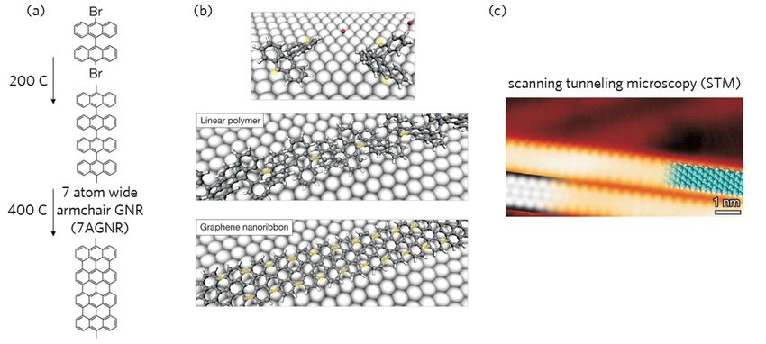
2 Bottom-up chemical synthesis of graphene nanoribbons The interest of opening the band gap in graphene quickly led to the fabrication of the first GNRs from bulk sheets of graphene or from CNTs. These GNRs were fabricated by either etching a bulk sheet of graphene down to thin strips or unzipping carbon nanotubes. While such “top- down” methods were successful at yielding semiconducting material, charge transport was hindered by the variation in width and edge structure along the GNRs as shown in Figure 2.1. The electronic structure and charge transport is so sensitive to the GNR structure, that even a few missing carbon atoms or adding an extra hydrogen atom at the end a 10 nm long GNR would completely change the electronic properties1,2. Addressing the lack of atomic control in the GNR would require a new fabrication technique that was developed in 2010. As shown in Figure 2.2, the technique yields GNRs with atomically precise edges and a uniform width along the ribbon which can be characterized with high resolution scanning tunnelling microscopy (STM). This chapter will discuss the details of the on-surface and solution grown GNRs and the recent advancements in the growth of GNRs with various electronic properties. Figure 2.1 | Top-down patterning of GNRs. (a) GNRs from lithography of bulk graphene and unzipping of CNTs3. (b) Scanning tunnelling microscopy image of a GNR from an unzipped CNT. Unzipping of GNRs causes rough edges that affect the electronic structure and degrade transport 4. The on-surface synthesis of GNRs starts in the synthetic chemistry lab, where a carefully chosen monomer is synthesized and purified. The monomer powder is then brought into an ultra- high vacuum (UHV) STM chamber where a metal crystal (or film) is cleaned to obtain an atomically smooth metal surface (typically Au(111)). The monomer is evaporated onto the metal surface and annealed, where it radicalizes from dehalogenation. Monomers diffuse along the surface and bond with each other to form polymers as shown in Figure 2.2. With another annealing step at a higher temperature, the polymers go under a process called cyclodehydrogenation. The polymer cyclizes into a flat, atomically smooth GNR by losing some of its hydrogens and forming new C-C bonds. This completes the synthesis. After this stage, various methods are used to 6
characterize the GNR in-situ, such as STM, scanning tunnelling spectroscopy (STS), and non-
contact atomic force microscopy (nc-AFM).

Figure 2.2 | Bottom-up chemical synthesis of 7AGNRs. (a) GNR precursor (DBBA) is evaporated
onto the Au surface, annealed to create a linear polymer, and annealed further to finalize the GNR
synthesis with cyclodehydrogenation. (b) 3D rendering of growth process on the Au surface. (c)
High resolution STM image of 7AGNRs showing uniform length and smooth, armchair edges 5.

 Since this process is performed under UHV conditions in a STM chamber, the sample can
be cooled down after each step and a high resolution STM image can be obtained as shown in
Figure 2.2. The edge structure and uniformity of the GNR is determined from the image. But to
prove that the GNR has the expected semiconducting density of states, STS is performed, which
will be discussed in Chapter 4. Some UHV systems used are equipped with a nc-AFM set-up which
takes images with remarkable bond-length resolution6. These images are more challenging to
obtain than typical STM images, but the payoff is clear proof that the GNR has the expected
molecular structure, as shown in the 9AGNRs in Figure 2.3.

 7
Figure 2.3 | Bond-length resolution images with non-contact AFM. (a) Room temperature STM
of 9AGNRs on Au(111). (b) non-contact AFM on 9AGNRs on Au(111) showing the pristine
9AGNR structure6.

 After the 2010 report of the first bottom-up synthesized GNR, many research groups around
the world raced to synthesize bottom-up GNRs as a platform for the study of novel physics and
chemistry or for integration in practical applications, such as FETs for logic systems. However, not
every monomer designed in the chemistry lab can be synthesized. Even if the monomer is
synthesized, the monomer may not behave as expected under UHV or on a surface and may not
grow GNRs. Finally, on-surface synthesis grows GNRs that are limited in length, which can hinder
the development of GNR devices. This led to the development of solution based GNR growth.

2.1 GNR precursor
 The chemical and physical properties of the monomer dictate whether the GNR growth will
be successful and what the resulting molecular structure of the GNR. Therefore, it has been a focus
to understand the synthesis of monomers that produce GNRs and the types of GNRs that these
monomers yield. This quest to build a monomer:GNR “library” is key for studying novel physics
with the GNRs as a platform and for the development of high-performance GNR devices. For
example, Figure 2.4 shows the first set of synthesized GNRs from monomers: 10,10’-dibromo-9,9’-
bianthryl (DBBA) which yields 7-atom wide armchair GNR (7AGNR) and 6,11-dibromo-1,2,3,4-
tetraphenlytriphenylene which yields the chevron GNR.

 8
Figure 2.4 | Various GNR precursors and the resulting GNR structure. (a) Armchair GNRs 3, 5,
7, 7 (B-doped), 9, 13 atoms wide. (b) Chevron-type GNRs with different nitrogen doping
configurations on the edges. (c) Zigzag-like edged GNRs7.

 While many different types of GNRs have been successfully synthesized using this technique,
there is a collection of potential GNR precursors that never grew any GNRs for various reasons:
First, after a candidate precursor is designed, it must be chemically synthesized. The fabrication of
some monomers requires multiple, challenging steps in their synthesis that can inhibit their yield
and final purification (i.e. not any monomer can be practically synthesized). Milligrams of
precursor material must be realized for the development of the on-surface GNR growth in UHV.
Second, the precursors must sublime at moderate temperatures (~200 C) under UHV conditions
without decomposing. Third, the monomer must land on the surface so that the reactive sites
where the halogen (Cl or I) sites line up as the monomer diffuses on the surface. If the halogen sites
of two monomers do not line up, the monomers may physically approach while diffusing on the
surface but will not polymerize due to misalignment of the reactive sites, also known as steric
hindrance. Fourth, the halogen must cleave off the monomer (dehalogenation) at a temperature
lower than cyclodehydrogenation (otherwise diffusivity goes to zero before the monomer can
polymerize) and the monomer must have some diffusivity on the surface at the dehalogenation
temperature. Ideally the cyclodehydrogenation temperature is much larger than dehalogenation
temperature so that the polymerization is not prematurely stopped by the cyclodehydrogenation 8.

 Once the monomer is on the surface, the temperatures of the dehalogenation,
polymerization, and cyclodehydrogenation must be low enough for the growth to occur without
desorption or decomposition of the monomer molecules. The temperatures required for growth
are mediated by the monomer’s interaction with the surface. Therefore, the choice of surface can

 9
determine whether the GNR grows, with metals being the most commonly used surface due to
their catalytic properties and the ability to perform STM on them.

2.2 Growth surface
 Different metal surfaces have been used for the growth of GNRs. The metal plays a critical
role in the growth by (1) efficiently adsorbing the precursor molecule, (2) catalyzing the
dehalogenation, (3) promoting surface diffusion of the monomers (templating the growth), and
(4) catalyzing the cyclodehydrogenation. Growths have been demonstrated on various metal
surfaces. Most notably, the low cost, wide availability, and favorable surface properties for GNR
growth of Au(111) has made it the metal of choice for most GNR growths. The Au(111) promotes
the growth of randomly oriented GNRs but Au can be engineered to template aligned growth. A
stepped, Au(788), surface can be obtained from a mis-cut single crystal Au to template the growth
of aligned GNRs9, as shown in Figure 2.5.

Figure 2.5 | Aligned 7AGNRs on Au(788). STM of templated, aligned 7AGNR growth on
Au(788)9.

 The availability of Au(111) thin films on Mica allows for growth on the sacrificial Au that
can be exploited for transfer to an insulating material, a critical step in device fabrication as
described in Chapter 5. Growing GNRs on an insulating surface has attracted attention over the
years because it would enable direct device fabrication on the growth surface, limiting the
possibility of GNR damage during the metal to insulator layer transfer.

 Growth on insulators has yet to be demonstrated, and it continues to be an active area of
research. Metals provide plenty of electrons that can promote the dehalogenation and
cyclodehydrogenation. Without all those free electrons on an insulator surface, the design of the
monomer should allow the dehalogenation to happen at a reasonable temperature (~200 C),
because molecules adhere less readily to the insulating surface causing the desorption temperature
of the molecules to drop significantly when compared to molecules sitting on metal. Furthermore,
cyclodehydrogenation temperature needs to be low without the presence of the metallic substrate.

 10
One strategy is to design the growth to avoid cyclodehydrogenation all-together, by growing a
monomer that polymerizes already conjugated, as some 5-atom wide GNRs (5AGNR) 10 grow as
shown in Figure 2.6. Even though there has been limited progress on growth on insulators, there
has been progress on understanding the growth kinetics on the surface which correlates to GNR
length.

Figure 2.6 | 5AGNRs grown on Au(111). (a) Synthesis of the GNRs using the 5AGNR precursor.
A single annealing step is needed since it polymerizes already planarized. (b) High resolution STM
of 5AGNRs grown and (c) High field of view STM image of 5AGNRs. The ribbons appear to grow
aligned along the herringbone reconstruction of the Au(111) surface 2.

2.3 Polymerization dynamics and improving length distribution
 Long GNRs (>100 nm) enable in-depth studies of the intrinsic GNR charge transport and
facilitate the integration of GNR devices into circuits. The yield of working GNR devices increases
dramatically as the average GNR length increases, as shown in Figure 2.7. However, bottom-up
GNR synthesis yields GNRs with lengths on the order of 10s of nanometers. The quality of the
precursor used and the growth dynamics on the surface inhibit the growth of long GNRs. If the
precursor molecules are not pure after isolation, there may be monomers on the surface with only
one halogen. The polymerization ends once the defective monomer reacts. Therefore, purifying
the precursor after synthesis as much as possible is critical in optimizing the length distribution of
the GNRs.

 11
Figure 2.7 | Length distribution from a typical GNR growth and device yield. (a) Calculated
device yield rises dramatically as GNR length increases. (b) Experimental length distribution of
9AGNRs grown on Au(111) using room temperature STM images like the one shown in (c).

 To further optimize GNR length, passivation of the precursor molecules during
polymerization must be minimized. Ideally, polymerization occurs without passivation of the
reactive sites in the monomers. Remnant hydrogen or other unwanted species in the UHV
chamber can limit polymer length by passivating the radicals 11. One proposed approach to
minimize this effect is to introduce a hydrogen getter, such as Ti or Co, near the growth surface to
decrease the hydrogen concentration. But improving GNR length by lowering hydrogen partial
pressure has yet to be demonstrated. A proven approach to improve length distribution is to
separate the temperatures of polymerization and cyclodehydrogenation 8.

 GNR length can be somewhat improved by optimizing the parameters in the growth
(temperatures and times of sublimation, polymerization, cyclodehydrogenation) 11. The stochastic
nature of polymerization and cyclodehydrogenation leads to a non-negligible amount of
cyclodehydrogenation occurring during polymerization. The polymerization temperature is
typically dominated by the temperature where the halogen cleaves off from the monomer, so to
increase the separation of polymerization and cyclodehydrogenation, the dehalogenation
temperature should be minimized. Iodine has been shown to cleave from the monomer more
readily on Au, thereby reducing the dehalogenation temperature and improving GNR length, as
shown in Figure 2.8. Further separation of these temperatures could potentially be realized by
 12
using a different metal surface that catalyzes dehalogenation more readily than
cyclodehydrogenation. Nevertheless, monomers are only able to move in two dimensions during
on-surface polymerization and may be trapped by adjacent, passivated molecules which makes
significant improvements in length distribution challenging. Moving the GNR growth to a solution
lifts the restrictive diffusion of the surface polymerization and removes the need to account for
steric hindrance during monomer design.

Figure 2.8 | Improving GNR length by replacing the halogen in the precursor molecule. (a)
9AGNR growth used to optimize length by changing the halogen in the X position of the precursor.
(b) GNR length distribution shows an improvement in average length with iodine as in the
monomer due to its lowered dehalogenation temperature 8.

2.4 Solution synthesis
 Solution synthesis of atomically precise GNRs followed the first on-surface growth of
7AGNRs12. Some of the first GNRs demonstrated with surface synthesis are shown on Figure 2.9.
The solution growth follows the same steps except for sublimation as its on-surface counterpart:
precursor design and synthesis, dehalogenation, polymerization, and cyclodehydrogenation.
Instead of a surface to template and catalyze the growth, GNRs that may not grow on a surface,
due to steric hindrance of the monomers, will readily grow in solution, with the assistance of
catalysts. This expands the GNR library by introducing new types of GNRs unattainable from
surface reactions. Furthermore, growth kinetics in three dimensions are more favorable for
realizing long polymers. Indeed, long GNRs (50-100 nm) have been demonstrated by solution
synthesis12,13.

 13
Figure 2.9 | Solution synthesis of chevron type GNR. Similar to on-surface growth, GNRs can be
polymerized and cyclized in solution by employing the use of catalysts in solution 12.

 While running the reaction in a solution prevents atomic resolution imaging via in-situ
STM, other avenues of manipulation characterization are opened. For instance, long polymers can
be sorted and purified by using common polymer chemistry techniques such as column
chromatography13, and the optical properties of suspended GNRs in solution can be characterized
with optical absorption and photoluminescence-emission measurements. However, on-surface
characterization of solution synthesized GNRs is elusive mainly due to the challenges in
suspending the GNR in solution and the deposition of isolated GNR or well dispersed GNR
networks on a surface.

 Solution GNRs are attractive for device applications for the reasons described above and for
their scalability. Scaling the growth to produce milligrams or grams of GNRs is much simpler done
in solution than on a surface in UHV conditions. However, GNRs interact strongly with each other
in solution (even more than CNTs due to GNR-GNR pi-pi stacking and the mechanical flexibility
of GNRs), and weakly with surfaces. The most common GNRs grown in solution also suffer from
a wide band gap14. As will be described in the next chapters, the development of high-performance
devices is impeded by the wide band gap of bottom-up GNRs. While there has been moderate
progress in the manipulation and deposition of solution based GNRs, the device behavior is poor
and the on-surface characterizations, such as STM, are inconclusive 15,16. The development of
solution GNR devices and studies of the GNR electronic properties will require new approaches
for the manipulation and deposition of solution GNRs.

2.5 Growth of GNR heterostructures
 If different types of GNR precursors are introduced in the growth, the monomers sometimes
copolymerize, resulting in GNRs made up of the covalently bonded GNR sections corresponding

 14
to each type of monomer used. On a surface, this means evaporating two different kind of
monomers before polymerization17,18. For example, 7AGNR and 13AGNR monomers can be co-
deposited on Au(111) and annealed to yield 7-13 heterostructures 17 such as the one shown in
Figure 2.10. Key factors for a successful heterojunction growth are the dehalogenation and
cyclization temperatures of the individual GNR components as well as the position of the halogens.
If one section cyclizes before the other section has the opportunity to copolymerize, the GNRs will
grow independently without interacting. Similarly, if the radical locations do not align on the
surface due to steric hindrance, the GNRs will also grow without forming heterojunctions. Finally,
this co-deposition technique leads to random co-polymer section lengths which may not be ideal
for device design and fabrication. Progress has been made to control the length of the subunits 19,
but the GNRs remain too short for device integration.

Figure 2.10 | STM of 7-13 AGNR heterostructures. (a) Synthesis of 7-13 AGNR heterojunction
involves co-deposition of the 7AGNR and the 13AGNR monomer. (b) STM image of a 7-13-7
quantum dot created by co-deposition and growth17.

2.6 Conclusions
 Bottom-up chemical synthesis can be used to produce GNRs with precision at the molecular
level. The GNR structure is determined by the monomer synthesized and purified. Various types
of GNR structures have been realized using bottom-up synthesis. GNRs can be grown either in
solution, with soluble catalysts introduced, or a surface, with the surface catalysing the growth. On
a surface, the metal surface can template the growth and determine the structure of the GNR.
Finally, if monomers of different types are introduced, the GNR heterostructures can form, which
are promising for novel (opto)electronic device applications. For the study and development of
GNR devices, GNRs must be transferred to an insulator and contacted with metal electrodes, as
presented in the next chapter.

 15
2.7 References
1. Talirz, L., Söde, H., Kawai, S., Ruffieux, P., Meyer, E., Feng, X., Müllen, K., Fasel, R., Pignedoli, C. A. &
 Passerone, D. Band Gap of Atomically Precise Graphene Nanoribbons as a Function of Ribbon Length and
 Termination. ChemPhysChem 20, 2348–2353 (2019). https://doi.org/10.1002/cphc.201900313
2. Lawrence, J., Brandimarte, P., Berdonces-Layunta, A., Mohammed, M. S. G., Grewal, A., Leon, C. C., Sánchez-
 Portal, D. & de Oteyza, D. G. Probing the Magnetism of Topological End States in 5-Armchair Graphene
 Nanoribbons. ACS Nano 14, 4499–4508 (2020). https://doi.org/10.1021/acsnano.9b10191
3. Segawa, Y., Ito, H. & Itami, K. Structurally uniform and atomically precise carbon nanostructures. Nature
 Reviews Materials 1, 15002 (2016). https://doi.org/10.1038/natrevmats.2015.2
4. Zhang, X., Yazyev, O. V., Feng, J., Xie, L., Tao, C., Chen, Y.-C., Jiao, L., Pedramrazi, Z., Zettl, A., Louie, S. G.,
 Dai, H. & Crommie, M. F. Experimentally Engineering the Edge Termination of Graphene Nanoribbons. ACS
 Nano 7, 198–202 (2013). https://doi.org/10.1021/nn303730v
5. Cai, J., Ruffieux, P., Jaafar, R., Bieri, M., Braun, T., Blankenburg, S., Muoth, M., Seitsonen, A. P., Saleh, M.,
 Feng, X., Müllen, K. & Fasel, R. Atomically precise bottom-up fabrication of graphene nanoribbons. Nature
 466, 470–473 (2010). https://doi.org/10.1038/nature09211
6. Talirz, L., Söde, H., Dumslaff, T., Wang, S., Sanchez-Valencia, J. R., Liu, J., Shinde, P., Pignedoli, C. A., Liang, L.,
 Meunier, V., Plumb, N. C., Shi, M., Feng, X., Narita, A., Müllen, K., Fasel, R. & Ruffieux, P. On-Surface
 Synthesis and Characterization of 9-Atom Wide Armchair Graphene Nanoribbons. ACS Nano 11, 1380–1388
 (2017). https://doi.org/10.1021/acsnano.6b06405
7. Talirz, L., Ruffieux, P. & Fasel, R. On-Surface Synthesis of Atomically Precise Graphene Nanoribbons. Adv.
 Mater. 6222–6231 (2016). https://doi.org/10.1002/adma.201505738
8. Di Giovannantonio, M., Deniz, O., Urgel, J. I., Widmer, R., Dienel, T., Stolz, S., Sánchez-Sánchez, C.,
 Muntwiler, M., Dumslaff, T., Berger, R., Narita, A., Feng, X., Müllen, K., Ruffieux, P. & Fasel, R. On-Surface
 Growth Dynamics of Graphene Nanoribbons: The Role of Halogen Functionalization. ACS Nano 12, 74–81
 (2018). https://doi.org/10.1021/acsnano.7b07077
9. Linden, S., Zhong, D., Timmer, A., Aghdassi, N., Franke, J. H., Zhang, H., Feng, X., Müllen, K., Fuchs, H., Chi,
 L. & Zacharias, H. Electronic Structure of Spatially Aligned Graphene Nanoribbons on Au(788). Phys. Rev. Lett.
 108, 216801 (2012). https://doi.org/10.1038/ncomms10177
10. de Oteyza, D. G., García-Lekue, A., Vilas-Varela, M., Merino-Díez, N., Carbonell-Sanromà, E., Corso, M.,
 Vasseur, G., Rogero, C., Guitián, E., Pascual, J. I., Ortega, J. E., Wakayama, Y. & Peña, D. Substrate-
 Independent Growth of Atomically Precise Chiral Graphene Nanoribbons. ACS Nano 10, 9000–9008 (2016).
 https://doi.org/10.1021/acsnano.6b05269
11. Fairbrother, A., Sanchez-Valencia, J.-R., Lauber, B., Shorubalko, I., Ruffieux, P., Hintermann, T. & Fasel, R.
 High vacuum synthesis and ambient stability of bottom-up graphene nanoribbons. Nanoscale 9, 2785–2792
 (2017). https://doi.org/10.1039/C6NR08975E
12. Vo, T. H., Shekhirev, M., Kunkel, D. A., Morton, M. D., Berglund, E., Kong, L., Wilson, P. M., Dowben, P. A.,
 Enders, A. & Sinitskii, A. Large-scale solution synthesis of narrow graphene nanoribbons. Nat Commun 5,
 (2014). https://doi.org/10.1038/ncomms4189
13. von Kugelgen, S., Piskun, I., Griffin, J. H., Eckdahl, C. T., Jarenwattananon, N. N. & Fischer, F. R. Templated
 Synthesis of End-Functionalized Graphene Nanoribbons through Living Ring-Opening Alkyne Metathesis
 Polymerization. J. Am. Chem. Soc. 141, 11050–11058 (2019). https://doi.org/10.1021/jacs.9b01805

 16
14. Radocea, A., Sun, T., Vo, T. H., Sinitskii, A., Aluru, N. R. & Lyding, J. W. Solution-Synthesized Chevron
 Graphene Nanoribbons Exfoliated onto H:Si(100). Nano Lett. (2016).
 https://doi.org/10.1021/acs.nanolett.6b03709
15. Abbas, A. N., Liu, G., Narita, A., Orosco, M., Feng, X., Müllen, K. & Zhou, C. Deposition, Characterization, and
 Thin-Film-Based Chemical Sensing of Ultra-long Chemically Synthesized Graphene Nanoribbons. J. Am.
 Chem. Soc. 136, 7555–7558 (2014). https://doi.org/10.1021/ja502764d
16. Abbas, A. N., Liu, B., Narita, A., Dössel, L. F., Yang, B., Zhang, W., Tang, J., Wang, K. L., Räder, H. J., Feng, X.,
 Müllen, K. & Zhou, C. Vapor-Phase Transport Deposition, Characterization, and Applications of Large
 Nanographenes. J. Am. Chem. Soc. 137, 4453–4459 (2015). https://doi.org/10.1021/ja513207e
17. Chen, Y.-C., Cao, T., Chen, C., Pedramrazi, Z., Haberer, D., Oteyza, D. G. de, Fischer, F. R., Louie, S. G. &
 Crommie, M. F. Molecular bandgap engineering of bottom-up synthesized graphene nanoribbon
 heterojunctions. Nat Nano 10, 156–160 (2015). https://doi.org/10.1038/nnano.2014.307
18. Cai, J., Pignedoli, C. A., Talirz, L., Ruffieux, P., Söde, H., Liang, L., Meunier, V., Berger, R., Li, R., Feng, X.,
 Müllen, K. & Fasel, R. Graphene nanoribbon heterojunctions. Nat Nano 9, 896–900 (2014).
 https://doi.org/10.1038/nnano.2014.184
19. Bronner, C., Durr, R. A., Rizzo, D. J., Lee, Y.-L., Marangoni, T., Kalayjian, A. M., Rodriguez, H., Zhao, W.,
 Louie, S. G., Fischer, F. R. & Crommie, M. F. Hierarchical On-Surface Synthesis of Graphene Nanoribbon
 Heterojunctions. ACS Nano 12, 2193–2200 (2018). https://doi.org/10.1021/acsnano.7b08658

 17
3 GNR transfer and device fabrication
 The GNR growth method, quality, and desired device configuration determine the best
strategy for the device fabrication process. GNR placement onto an insulating surface (transfer)
and contact with patterning techniques are the two critical steps in the device fabrication process.
A layer transfer technique can be employed for placing GNRs on an insulating surface after growth
on a metal surface1–3. Solution deposition techniques can be employed to place GNRs on any
surface, albeit with limited success so far due to GNR aggregation. After placement, a GNR is
contacted at each end for individual-GNR devices or bulk GNR films are contacted for thin film
devices. The required feature size is usually dependent on the GNR length for single GNR devices.
For example, the fabrication of a single-GNR devices using the surface growth process will require
a layer transfer process to an insulator as well as patterning of contacts with ~20 nm gaps, due to
the short length (10s of nanometers) of these GNRs. In contrast, feature size constraints are relaxed
for the fabrication of devices with large scale GNR or CNT films that cover large areas (100s of
micrometers) allowing for contact gaps that can be as large as 10s of micrometers. While the
fabrication of thin film devices is significantly simpler, characterization of single-GNR nanoscale
devices are critical in the understanding the intrinsic electron transport of GNRs and developing
high-performance FETs.

 In this chapter, the device fabrication of individual-GNR devices is described. As illustrated
in Chapter 2, GNRs can be grown on Au(111) and imaged in-situ with high resolution STM.
Unfortunately, resolving single-GNR has not been achieved once the sample is removed from the
UHV chamber and transferred to an insulating surface. The short GNR length, GNR transfer, and
inability to image individual GNRs are the main challenges in the device fabrication process. To
overcome these challenges, GNRs are grown on a thin Au(111) film that can be used as a sacrificial
and mechanical support layer during transfer to the device substrate. Then 100s of electrode pairs
with ~20 nm spacing are patterned on the transferred region and probed in the search for a GNR
in the electrode gap. This type of shotgun approach is commonly used in molecular electronics
where individual molecules are also difficult to locate 4.

 First, large patterns, such as the pads used for electrical probing, are patterned using optical
lithography. Then, GNRs are transferred from their growth substrate and, finally, nanoscale
contacts are patterned via electron beam lithography.

3.1 Optical lithography of the device substrate
 The semiconductor industry has used optical lithography for the patterning and fabrication
of integrated circuits for decades. In an academic lab, deep UV lithography steppers provide
patterning with a resolution of ~200 nm. Our finest feature size is the source-drain gap that must
be smaller than the GNR length, which is on the order of ~20 nm and must be patterned with

 18
You can also read