Residual polymer stabiliser causes anisotropic conductivity in metal nanoparticle 2D and 3D printed electronics - Research Square
←
→
Page content transcription
If your browser does not render page correctly, please read the page content below
Residual polymer stabiliser causes anisotropic
conductivity in metal nanoparticle 2D and 3D
printed electronics
Gustavo F. Trindade*1,2, Feiran Wang2, Jisun Im2, Yinfeng He2, Adam Balogh2,
David Scurr1, Ian Gilmore3, Mariavitalia Tiddia3, Ehab Saleh2,4, David Pervan2,
Lyudmila Turyanska2, Christopher J. Tuck2, Ricky Wildman2, Richard Hague2,
Clive J. Roberts*1
1
  Advanced Materials and Healthcare Technologies, School of Pharmacy, University of
Nottingham, University Park, Nottingham, NG7 2RD, UK
2
  Centre for Additive Manufacturing, Faculty of Engineering, University of Nottingham, Jubilee
Campus, Nottingham, NG7 2RD, UK
3
  National Physical Laboratory, Hampton Road, Teddington TW11 0LW, UK
4
  School of Chemical and Process Engineering, University of Leeds, Leeds, LS2 9JT, UK

*CORRESPONDING        AUTHOR(S):
Gustavo.FerrazTrindade@nottingham.ac.uk and Clive.Roberts@nottingham.ac.uk

ABSTRACT: Inkjet printing of metal nanoparticles (MNPs) allows for design flexibility,
rapid processing and enables 3D printing of functional electronic devices through co-
deposition of multiple materials. However, the performance of printed devices, especially
their conductivity, is lower than those made by traditional manufacturing methods and is
previously not fully understood. Here, we revealed that anisotropic electrical conductivity
of printed MNPs is caused by organic residuals from MNPs inks. We employed a
combination of electrical resistivity tests, morphological analysis and novel 3D nanoscale
chemical analysis of printed devices using silver nanoparticles (AgNPs) to show that the
polymer stabiliser polyvinylpyrrolidone (PVP) tends to concentrate between vertically
stacked AgNPs layers as well as at dielectric/conductive interfaces. The understanding
of organic residues behaviour in printed nanoparticles reveal potential new strategies to
improve nanomaterial ink formulations for functional printed electronics.

                                                                                            1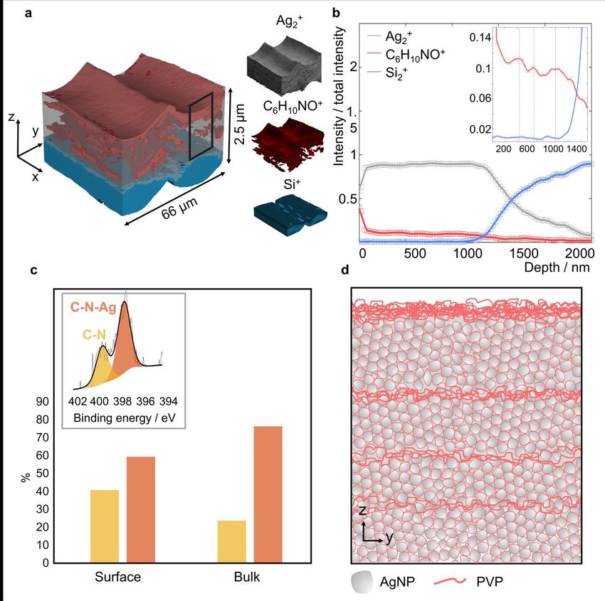
Introduction
  Digitally printed electronics are a driver for novel research in various fields owing to their
design flexibility as well as other advantages such as expedited time-to-market.1–3 Ink
jetting of inks containing colloidal materials, such as metal nanoparticles (MNPs),4–8
germania-silica,9 and semiconductor quantum dots10 has been successfully employed in
applications ranging from flexible and wearable electronics11–19 to quantum optoelectronic
devices20–22 and fully printed perovskite solar cells.23–26 However, the performance of
printed parts is not competitive with those made by traditional manufacturing methods.
This is due to challenges in both manufacturing techniques and choices of materials, of
which there is a lack of comprehensive understanding. MNPs are among the most
commonly used conductive materials for printed electronics, and typically require
consolidation via a two-step process: solvent evaporation upon printing (pinning) and
subsequent low-temperature sintering (120–200 °C),4,14,27–30 enabling conductive tracks
on polymer substrates.4,7,13 More recently, inkjet-based 3D printing has been used to
enable the selective co-deposition of different functional materials contemporaneously
(i.e. dielectric and/or conductive materials),4,5,27,31–33 to ultimately achieve the production
of macroscopic multi-material objects with multiple functionalities.
  Despite significant interest in utilising MNP-based materials in 2D and 3D printed
electronic devices, the lower and anisotropic intra-layer (planar) and inter-layer (vertical)
conductivity of MNP layers, compared to bulk metals, limits device performance and
hence uptake in industry and products.4 The conductivity of MNPs layers are known to
be dependent on sintering temperature and have been previously attributed to
morphological changes and possible organic residues.4,30,34 However, the detailed
mechanism of low-temperature sintering of MNPs that leads to reduced conductivity
remains to be fully understood.
  Organic molecules are used in MNPs inks as stabilisers or capping agents to enable
particle dispersion in low viscosity solvents, however, their residues are likely to hinder
device performance,34 even when present in very small amounts. Surface sensitive
chemical analysis techniques of time-of-flight secondary ion mass spectrometry (ToF-
SIMS) and X-ray photoelectron spectroscopy (XPS), in combination with gas cluster ion
beams (GCIBs), are a powerful toolset for depth profiling organic materials with high

                                                                                              2
chemical specificity, sensitivity, and nanometre depth resolution,35–42 chemical imaging of
buried hybrid organic/inorganic interfaces43,44 and characterisation of core-shell
structures.45–51
  Here, we present a comprehensive study of the effect of the organic residues, such as
stabilisers, and their localised distribution at the interface between printed layers on the
functional performance of the printed devices before and after low-temperature sintering.
Our results provide new insights on routes to improve intra-layer AgNPs sintering and
overcome functional anisotropy and hence improve uptake of this potential
transformational technology. Our methodology is transferable to other nanomaterial-
based inks and relevant for the development and exploitation of both 2D and 3D printed
electronics.

Results
Distribution of polymer stabiliser upon printing of AgNPs
  To investigate the interface of AgNPs during the inkjet printing and pining process, we
carried out high resolution chemical analysis of samples under a selection of printing
conditions. As a result, we have found polyvinylpyrrolidone (PVP) on the surface of
printed layers of AgNPs by means of the unambiguous identification of characteristic PVP
signal36,52 using a novel 3D orbiSIMS instrument53 and XPS (Fig. 1 and Supplementary
Fig. S1). PVP is a commonly used stabiliser, reducing agent, and shape-controlling agent
for the synthesis of metal nanoparticles.54,55 As a capping agent, it makes MNPs disperse
well in aqueous and organic solvents due to its amphiphilic characteristics derived from
the highly polar amide group within the pyrrolidone ring and hydrophobicity from the
methylene backbone. PVP thus plays a vital role in dispersing and stabilising the MNPs
in the solvents for stable ink formulation.56 However, PVP does not completely
decompose under typical multi-material jetting and sintering temperatures (up to 150°C)5
and its residues are likely to remain. Understanding the state and distribution of PVP upon
inkjet printing and post-deposition treatment of AgNPs is essential to develop solutions
that minimise its impact on the performance of printed electronics.

                                                                                          3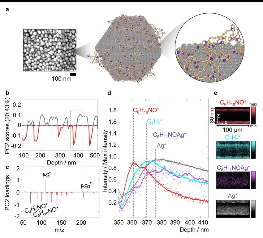
Fig. 1 inkjet printing AgNPs and detection of polymer stabiliser. a Drop-on-demand jetting of
inks containing AgNPs with in-situ solvent evaporation (pinning). b Optical image (bottom) of a
printed layer of AgNPs and chemical maps (top) showing the distribution of Ag2+ (grey), C6H10NO+
(red) and Si+ (blue) at the surface of a printed layer, c pair of deposited droplets and d two
coalesced droplets. The line plots represent the intensity across the centre of each map.

  Inkjet printing of AgNPs starts with printing and then pinning the material by removing
the solvent (Fig. 1a). All printing was conducted on a hot stage at 90 °C, which is sufficient
for pinning the printed ink without triggering AgNPs sintering. This temperature is also low
enough to prevent printhead damage and polymeric substrate degradation. The chemical

                                                                                              4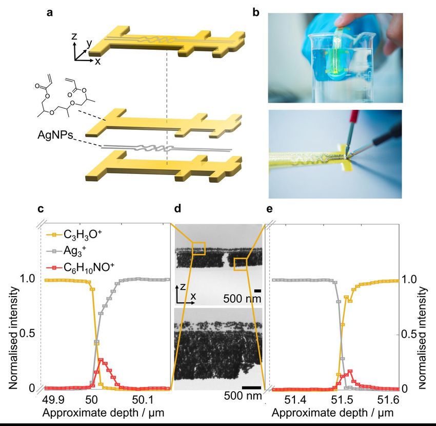
mapping data from the top surface of a printed layer of AgNPs (Fig. 1b) and individually
deposited droplets (Fig. 1c-d) show a ‘coffee ring’ effect where the solute (PVP) and
suspending MNPs tend to flow towards its pinned contact line following the outward flow
initiated by the combination of evaporation and contact-line pinning effect.57,58 This is
observed as a pattern with PVP-rich lines at the edge of each swath of MNPs ink across
the entire surface(Fig. 1b).57,59 The presence of PVP, even if at very low concentrations,
can hinder the sintering of MNPs at the interface, leading to reduced conductivity in the
inter-layer (vertical) direction.4 In a 3D printing context, subsequently deposited AgNPs
layers will therefore encounter a PVP-rich surface and these organic molecules may
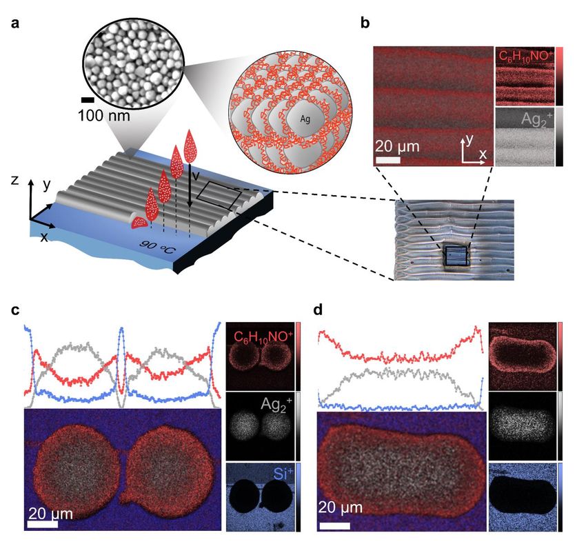
become trapped at the interface. We examined the three-dimensional distribution of PVP,
via ToF-SIMS depth profiling, within a sample consisting of four successively printed
layers of AgNPs ink. The results (Fig. 2a-b) show that the top surface has the strongest
PVP signal intensity, and that PVP signal was also detected through the bulk. Moreover,
the PVP intensity oscillates with an average period of 282.8 nm and peaks at
approximately 300, 600 and 900 nm depth (confirmed by fast Fourier transforms in
Supplementary Fig. S5a) which, based on the single layer data (Supplementary Fig. S2),
are the depths at which printed layer interfaces are expected to be located. This is
consistent with our hypothesis that PVP concentrates at the interface between printed
layers (Fig. 2d) and suggests that this happens during the layer-wise printing process.
5Fig. 2 3D chemical analysis of 4 stacked layers of inkjet 3D printed AgNPs. a 3D rendering of
ToF-SIMS signal for Ag2+, C6H10NO+ and Si+. b Depth profile (averaged over an area of 50 × 50
µm2 per depth level) showing accumulation of PVP at layers interface. c XPS N1s data for non-
interacting, free (C-N, 400 eV) and interacting (C-N-Ag, 398 eV) PVP with the Ag surface on top
surface and bulk (~100 nm deep).d Illustration of cross-section of stacked AgNPs layers with
PVP-rich interfaces.
The high resolution XPS spectrum of N1s of the printed AgNPs (Fig. 2c) shows that the
non-interacting form of PVP, presumably unbound PVP residues in the ink, (represented
6by C-N at 400 eV) is more abundant at the top surface, whilst the interacting form
(represented by C-N-Ag at 398 eV) has a stronger signal in the bulk (~100 nm deep).60
This, in conjunction with the ToF-SIMS depth profile (Fig. 2b), indicates that non or
weakly-interacting PVP tends to migrate to the outer surface of the ink, forming a thin
coating on the top surface upon solvent evaporation (Fig. 2d). However, non or weakly
interacting PVP was also detected in between printed layers with relatively high intensity.
In order to obtain enhanced depth resolution of chemical information within the printed
material, we carried out ToF-SIMS depth profiling using a lower beam energy and lower
current for the etching ion beam (Fig. 3) (details in Methods). Principal component
analysis (PCA) using depth levels as observations and a list of peaks as variables (Fig.
3b-c PC 2 with 20.43% of total variance – full PCA results are in Supplementary Fig. S4)
revealed a secondary, more complex, oscillating pattern within a single printed layer with
an average period of 80.7 nm (confirmed by fast Fourier transforms in Supplementary
Fig. S5b), which is compatible with the average diameter of individual silver nanoparticles
in the ink (60±22 nm, Supplementary Fig. S3). The slightly higher length is attributed to
nanoparticles packing and the oscillating pattern alternates between characteristic ions
for silver (such as Ag+, 109Ag+ and Ag2+) and PVP (such as C4H6NO+ and C6H10NO+). We
interpret that this is related to the core-shell structure of AgNPs/PVP and the irregularities
in the signal arise from the average PVP distribution on the surface of several Ag
nanoparticles within the ToF-SIMS analysis area.
In this nanoparticle-resolution depth profile, we tracked the signal of more specific
secondary ions related to the cyclic amide of pyrrolidone (C6H10NO+), linear hydrocarbon
(C4H7+), the cyclic amide-silver (C4H6NOAg+) and silver (Ag+) and normalised their signals
by their maximum intensity (Fig. 3d-e). We observed that each ion signal peaks at
different depths, revealing molecular-level information. These results give evidence of the
interaction of PVP with the AgNPs surface (Fig. 3a), in agreement with what has been
previously predicted via molecular dynamics simulations61–64. Every data point in the ToF-
SIMS depth profile represents only the first few nanometres of that depth level.; moreover,
none of the secondary ion intensities decrease to zero within an oscillation, which is
related to the fact that the capping polymer is present on the surface of all silver
nanoparticles.
7Fig. 3 PVP coordination onto AgNPs surface. A SEM micrograph of printed AgNPs and
schematic showing PVP coordination on a single AgNP surface. b PCA scores and c loadings of
depth profiling data at nanoparticle depth resolution. The dashed rectangle represents d depth
profile within 100 nm showing signals for secondary ions C6H10NO+, C4H7+, C6H11NOAg+ and Ag+.
e XZ maps within a depth of 80 nm. The data is averaged over an area of 100 x 100 µm2 per
depth level.
Influence of sintering temperature on the distribution of residual
polymer stabiliser and electrical resistivity
8Sintering is a commonly used post process to promote inter-particulate bridging as well
as the removal of residual organics. To evaluate how this process affects chemical,
morphological and electrical properties of printed samples, the AgNPs were deposited
and pinned as both single-layer and 200 layers electrodes and post-processed in an oven
at different temperatures (T) up to 500 ºC. The resistivity of all samples was measured at
room temperature (Fig. 4a,b,d), while their morphology was assessed by electron
microscopy (Fig. 4c and Supplementary Fig. S6). The planar resistivity (ρxy) of the sample
with a single printed layer decreased dramatically after processing at 100 oC and the
resistivity remains ~13 µΩ∙cm for the samples sintered at the temperatures ranging from
100 oC to 200 oC. Micrographs of AgNPs show that the particles start bridging around
these temperatures (Fig. 4c.i,ii), hence forming conductive channels and leading
to resistivity reduction. We noticed that ρxy of the single
layer printed AgNP samples remains about one order of magnitude higher than expected
for bulk silver (black dashed line in Fig. 4d). A further increase of processing temperature
to above 300 ºC results in an unexpected increase of ρxy for the single-layered samples
due to inter-particle voids with diameters between 200 and 500 nm shown in
Fig. 4c.iii. When the AgNPs were processed at 500 ºC, the AgNPs agglomerated into
macro structures sized 1 to 5 µm with very poor continuity (Fig. 4c.iv). For multi-layer
samples (200 layers), the stacking of layers filled the voids and thus avoided the
deterioration of conductivity pathways to keep the planer resistivity in the range of 10
µΩ∙cm for all samples treated at high temperatures to 500 oC. However, the vertical
resistivity of 200 layers (ρz) is about up to three orders of magnitude higher (23560±8350
µΩ∙cm for samples treated at T = 130 ºC) than ρxy. We employed XPS and ToF-SIMS to
detect residual PVP at the surface of printed AgNPs after processing (Fig. 4e-h). The
results show that PVP is still present after sintering the printed samples at temperatures
between 100 and 230 ºC, where resistivity is heavily anisotropic. Moreover, the proportion
of non-interacting PVP (normalised ratio between XPS N1s peaks at 400 eV and 398 eV,
Fig. 4e) increases with processing temperatures at the top surface but decreases in the
bulk (~100nm deep). This confirms the hypothesis that weakly interacting PVP migrates
to the surface (or layer interface in multi-layer samples) during sintering. These results
also agree with thermal gravimetric analysis results that show a 70% weight loss between
9the temperatures of 150ºC and 250 ºC, from solvent evaporation (available in
Supplementary, Fig. S7).
Fig. 4 Surface analysis, resistivity, and morphology of AgNPs printed and sintered at
different temperatures. Schematic of a single layer and b multi-layer inkjet printed AgNPs
10electrodes for planar and vertical resistivity measurements. c Secondary electron micrographs of
electrodes sintered at different temperatures: i. 25ºC, ii. 200ºC, iii. 300ºC and iv. 500ºC. d Results
of planar (ρxy) and vertical (ρxy) resistivity tests for single-layer and 200-layers samples sintered
at different temperatures. e Percentage of non-interacting PVP (from XPS) at the surface and
bulk for samples treated at different temperatures. f Characteristic ToF-SIMS secondary ions for
PVP (C6H10NO+), silver (Ag+) and the substrate (Si+) and XPS C1s peak-fitted52 components N-
C=O + C-N in function of sintering temperature. g XPS C1s peak fitting for sample at 25 oC and
h XPS N1s peak fitting for samples at 25 oC and 230 oC. Details of the XPS peak-fitting parameters
can be found in Supplementary Tables ST1 and ST2.
Residual PVP in a multi-material 3D printed device
We applied the same methodology to map residual PVP within a fully 3D printed
encapsulated strain sensor that was produced via multi-material inkjet printing (Fig. 5a-
b). The conductive channel consists of 5 printed layers of AgNPs processed using UV
light and the dielectric material is tri(propylene glycol)diacrylate (TPGDA), represented by
the secondary ion C3H3O+. Details about the device and printing method are reported in
our previous work.4,43 As both the dielectric and conductive layers are printed
contemporaneously, temperatures for in-situ or post-processing must remain low to avoid
damaging the organic material. Moreover, the glass transition temperature (Tg) of PVP is
in the range 100~150 oC, depending on its molecular weight55,65,66, which may lead to
migration of PVP within the surface and interface of AgNPs during the post-processing
sintering.67 Chemical depth profiling results (Fig. 5c,e) show that residual PVP is present
at higher quantities at the dielectric/conductive materials interface, in agreement with the
results shown in Fig. 2, where greater signal of PVP was detected at the top surface of
AgNPs printed layers. The presence of organic residues at the interface between
contemporaneously deposited materials is potentially deleterious to device performance
where, specifically for this case, it may influence adhesion between the organic and
inorganic materials. Furthermore, at the top TPGDA/AgNPs interface (Fig. 5c), silver is
detected earlier in the depth profile than PVP. This is explained by TEM micrographs of
a cross section of the device (Fig. 5d), which show interpenetration of AgNPs into the
dielectric material. This is not observed at the bottom interface (Fig. 5e) because of the
11order in which materials are deposited: AgNPs deposited on a solidified layer of organic
material have less mobility than when a liquid organic material is deposited onto a layer
of AgNPs.
Fig. 5 Presence of residual stabiliser in a multi-material inkjet 3D printed encapsulated
strain sensor. a Schematic showing the layer structure of the device. b photographs showing
that encapsulation enables the use of the device under water. ToF-SIMS depth profile results at
12the c top and e bottom interface. The dielectric material is TPGDA and represented by C3H3O+.
PVP is represented by C6H10NO+ d TEM micrographs of a cross section.
Discussion
We showed that poor inter and intra-layer electrical conductivity in silver structures
produced via 3D inkjet printing of AgNPs results from a combined chemistry and
morphology interface evolution during the low-temperature sintering process. This has
been achieved via the determination of the 3D spatial distribution of residual polymeric
capping agents within multiple printed layers. The residual polymer leads to anisotropic
conductivity reduction as we showed that such organic residues accumulate at the
interface of vertically stacked printed layers. With a clearer understanding of the
distribution of residual organic stabiliser within the printed layers, it is possible to consider
optimisation strategies to overcome the functional anisotropy of inkjet-based 3D printed
electronics. When printing multiple layers, it is not practical to remove the part from the
printer after each layer, especially when multiple materials are deposited
contemporaneously (Fig. 5). In that case, post-processing strategies should be converted
into in-situ processing steps. When working with commercially available nanoparticulate
ink formulations, the presence of a polymer stabiliser such as PVP is often inevitable,
which therefore requires additional post processing methods to overcome functional
anisotropy. We showed that higher sintering temperatures are not always beneficial, not
only because of potential damage to the substrate or contemporaneously deposited
materials, but also because AgNPs tend to coalesce, resulting in further planar
conductivity reduction. Silver nanoparticles have been proven to be sintered with
ultraviolet (UV) and infrared (IR) light, which makes it the most likely processing route for
printing 3D macrostructures,4,30 therefore, the understanding of how a stabiliser behaves
upon printing and sintering of metal nanoparticles is essential to aid ink formulation routes
with different stabilisers that can either be removed at lower temperatures or be breakable
upon excitation using UV or IR sources.68
Methods
13AgNPs ink used in this work was purchased from Advanced Nano Products (SilverJet
DGP-40LT-15C) and was used as-received. The nominal composition of the ink consists
of 38.85 wt% of silver nanoparticles dispersed in triethylene glycol monomethyl ether
(TGME) and other additives. Thermogravimetry analysis (TGA) and differential scanning
calorimetry (DSC) of silver NP inks were performed simultaneously on a TA Q600 unit.
The sample ink was placed and dried in a vacuum oven at 40 °C prior to the
measurement. The sample was heated up at a temperature ramp of 10 °C min-1 under
constant nitrogen flow of 100 mlmin-1.
AgNPs samples were printed using a Fujifilm Dimatix Materials Printer DMP-2850
Series with a 10 pL cartridge. The droplet diameter is ~ 45 µm and a drop spacing
distance of 30 µm was used to ensure deposition of continuous layers and pattern
uniformity. Only one nozzle was employed to maximise the morphological homogeneity
and geometrical precision of deposition. The samples were printed on a Si/SiO2 substrate.
For all samples (apart of room temperature sample) the substrate was heated to 90 ºC by
an in-situ resistance heater.
The encapsulated strain sensor was inkjet 3D printed with co-deposition of the
AgNPs and an organic ink made in-house and based on tri(propylene glycol)diacrylate
(TPGDA). Both polymer and silver layers were printed and cured/sintered
contemporaneously by a LED-based UV source connected to the print-heads of a PixDro
LP50 printer. This sample was used to benchmark a sample preparation methodology
previously published.43 More details of the ink formulations and printing method are
described elsewhere.4
The planar resistivity of printed AgNPs samples was measured using a Keithley
2400 sourcemeter and a Keithley 7500 multimeter with a four-probe method, also known
as Kelvin technique, to eliminate contact resistance. A voltage is applied from the two
probes at the ends and the current through the printed line was measured with the change
of voltage drop across the two probes in the middle. Each I-V curve was measured three
times using both forward and backwards scanning. The derivative of the I-V curve reveals
the conductivity of the printed line with the precise geometry measured by an optical
microscope. All measurements were repeated three times for at least three different
samples, and results are presented as an average value with its standard deviation.
14The vertical resistivity of multiple printed layers of AgNPs was measured by
printing two hundred layers of the silver nanoparticle ink on ITO glass at 90 oC for good
drying and pinning and sintering at 130 oC, 200 oC and 300 oC. A 125 µm thick PEN film
with a window of the same size and shape of the sample was put on top to expose the
top layers and insulate the bottom contacts from the top contact. A glass slide with a wire
and dried silver paste facing downwards are then pushed firmly on top of the sample and
the PEN film as the top contact. The I-V curve is then measured using a Keithly
sourcemeter to extract the resistance. From all measurements, we could still observe a
contact resistance for all samples. To work out the contact resistance, the same
procedures have been repeated for 50 printed layers. The sample thicknesses were
measured by SEM of cross sections. By subtracting the resistance of thinner samples,
the ρz values of different sintering temperatures can be obtained.
Scanning electron microscopy (SEM) was carried out using a JEOL 7100F FEG-
SEM instrument which uses an in-lens Schottky field emission source. The microscope
was operated a with a 5 keV electron beam and at a working distance of 5 mm. Samples
were mounted on an aluminium stub using double-sided conductive carbon tape. Image
analysis was done with ImageJ 1.49k.
Transmission electron microscopy (TEM) was carried out using a JEOL 2000 FX
TEM with a 200 kV electron beam. Thin cross-sections of the encapsulated strain sensor
were prepared using a diamond knife in an Ultramicrotome PowerTome (RMC Products).
Samples were embedded in epoxy resin before cutting.
X-rays photoelectron spectroscopy (XPS) was carried out using an AXIS ULTRA
instrument (Kratos) with a monochromated Al kα X-ray source (1486.6eV) operated at 10
mA emission current and 12 kV anode potential (120 W) Spectra were acquired with the
Kratos VISION II software. A charge neutraliser filament was used to prevent surface
charging. High-resolution spectra at pass energy 20 eV, a step of 0.1 eV, and sweep
times of 10 minutes each were also acquired for photoelectron peaks from the detected
elements and these were used to model the chemical composition. All spectra were
charge corrected to the C 1s peak (adventitious carbon / CH2) set to 284.8 eV. Peak fitting
of the C1s and N1s scans was performed on the Casa XPS software (www.casaxps.com)
15using mixed Gaussian/Lorenzian components. Details of the fitting parameters are in
Supplementary Tables ST1 and ST2.
Surface time-of-flight secondary ion mass spectrometry (ToF-SIMS) of AgNPs
samples treated at different temperatures was carried out using a ToF-SIMS IV
instrument (IONTOF GmbH). Secondary ion mass spectra were acquired in positive ion
polarity mode using a 25 keV Bi3+ primary ion beam delivering 0.3 pA. The primary ion
beam was raster scanned over different areas with the total ion dose kept under the static
limit of 1013 ions/cm2. The ToF analyser was set with 200 µs cycle time, resulting in a
mass range between 0 and 3492 mass units and a low-energy (20 eV) electron flood gun
employed to neutralise charge build up.
ToF-SIMS 3D mapping of AgNPs was carried out using a 3D OrbiSIMS (Hybrid SIMS)
instrument from IONTOF GmbH. The ToF-SIMS data were acquired in positive ion
polarity mode in dual-beam mode by raster scanning a 30 keV Bi3+ primary ion beam
(delivering 0.08 pA) of 100 × 100 µm2 at the centre of a 300 × 300 µm2 sputter crater
formed using an argon gas cluster ion beam (GCIB). The GCIB was operated in two
conditions, high-energy with 20 keV and 2000 atoms in the cluster with 5 nA beam current
and low energy using 10 keV and 1500 atoms per cluster delivering 3 nA. The analysis
was performed in the “non-interlaced” mode with a low-energy (20 eV) electron flood gun
employed to neutralise charge build up. For the low-energy settings, 3 sputter frames
were performed per cycle with 15 analysis scans per cycle and a pause time in between
cycles of 0.5 s. For the high-energy settings, 5 sputter frames were performed per cycle
with 20 analysis scans per cycle and a pause time in between cycles of 0.5 s. The ToF
analyser was set with 200 µs cycle time, resulting in a mass range between 0 and 2233
mass units.
ToF-SIMS depth profiling of multi-material device: was carried out using a ToF-
SIMS IV (IONTOF GmbH) in dual-beam mode by raster scanning a 25 keV Bi3+ primary
ion beam (delivering 0.08 pA) of 100 × 100 µm 2 at the centre of a 300 × 300 µm2 sputter
crater formed using a 20 keV argon gas cluster ion beam (GCIB) delivering 20 nA. The
analysis was performed in the “non-interlaced” mode with a low-energy (20 eV) electron
flood gun employed to neutralise charge build up. 5 sputter frames were performed per
cycle with 20 analysis scans per cycle and a pause time in between cycles of 0.5 s. The
16ToF analyser was set with 200 µs cycle time, resulting in a mass range between 0 and
2233 mass units. AgNPs/TPGDA interfaces were reached profiling from top and bottom
surfaces. To reach the buried interfaces, the etching beam current had to be greater and
acquisition time per level lower, which resulted respectively in limited depth resolution and
lower signal to noise ratio to be able to detect PVP within layers of AgNPs in a similar
manner to what is presented in Fig. 1 and Fig. 2).
ToF-SIMS data processing: All ToF-SIMS intensity maps were normalised by total ion
counts to correct for topographic features. All intensity maps were produced using the
simsMVA software.69 For 3D renders, voxel intensities were normalised by total ion
counts to account for topographic features and the z-scale was corrected based on the
substrate signal. The final 3D representations were created by combining rendered
isosurfaces ranging from 30% to 50% of the maximum intensity for each ion. Multivariate
analysis was carried out using the mass as the variables and each spectrum in the depth
profile sequence as the observations. For each depth profiling dataset, Surface Lab 7.1
(IONTOF GmbH) was used to perform an automated peak search on the total spectra
restricted only to peaks with intensity higher than 100 counts and masses between 30 u
and 300 u. Dead-time corrected peak areas were then exported for each sequential mass
spectrum in the depth profile. Principal component analysis (PCA) was performed using
the simsMVA software,69 which yields components loadings with groups of peaks that
shared the same depth profile (scores). Prior to PCA, data was Poisson scaled to account
for heteroscedasticity.70
Orbitrap secondary ion mass spectrometry (OrbiSIMS) was carried out using a 3D
OrbiSIMS (Hybrid SIMS) instrument.53 A 20 keV Ar3000+ GCIB of 20 µm diameter,
delivering 3.5 nA (with duty cycle set to 70.4%) was used as the primary ion beam. Depth
profiling data were acquired over areas of 300 × 300 μm2 using random raster mode with
crater size 382 × 382 μm2. The sample voltage was set at +57.5 V. Argon gas flooding
was used to aid charge compensation and the pressure in the main chamber was
maintained at 9.0 × 10⁻⁷ bar. The spectra were collected in positive polarity, in mass
range 50 - 750 m/z. Mass resolving power was 218,726 at 200 m/z.
Optical profilometry was used to determine the crater depth after ToF-SIMS depth
profiling experiments and calibrate the depth scale. Scans were obtained using a Zeta-
1720 optical microscope (Zeta Instruments) in a Z range of 4.6 µm. The number of steps
was set to 328, allowing for a z step size of 14 nm.
Acknowledgements
This work was funded by the Engineering and Physical Sciences Research Council
award: “Enabling Next Generation Additive Manufacturing” (grant number
EP/P031684/1). The authors acknowledge access to facilities at the Nanoscale and
Microscale Research Centre (nmRC) of the University of Nottingham and technical
support from Dr Emily Smith (XPS measurements), Ms Nichola Weston (assistance with
ultra-microtome and TEM) and Mr Martin Roe (assistance with the electron microscopy).
The EPSRC are gratefully acknowledged for the Strategic Equipment grant “3D
OrbiSIMS: Label free chemical imaging of materials, cells and tissues” funding that
supported this work (grant no. EP/P029868/1).
Authors contributions
GFT, FW, YH, CJT, RH and CJR conceived and planned the experiments. GFT carried
out the chemical characterisation, data analysis and interpretation supported by YH, JI,
DS, IG, MT, LT, RW, RH and CJR. GFT, AB and DP carried out electron microscopy.
FW, YH and AB produced all AgNPs samples. DP carried out the thermogravimetry
analysis. ES designed and produced the encapsulated strain sensor supported by CJT.
FW carried out the resistivity tests supported by JI, LT and CJT. All authors provided
critical feedback and wrote the manuscript.
References
(1) Kamyshny, A.; Magdassi, S. Conductive Nanomaterials for 2D and 3D Printed
Flexible Electronics. Chem. Soc. Rev. 2019, 48 (6), 1712–1740.
https://doi.org/10.1039/c8cs00738a.
(2) Ko, S. H.; Pan, H.; Grigoropoulos, C. P.; Luscombe, C. K.; Fréchet, J. M. J.;
18Poulikakos, D. All-Inkjet-Printed Flexible Electronics Fabrication on a Polymer
Substrate by Low-Temperature High-Resolution Selective Laser Sintering of Metal
Nanoparticles. Nanotechnology 2007, 18 (34). https://doi.org/10.1088/0957-
4484/18/34/345202.
(3) Lewis, J. A.; Ahn, B. Y. Three-Dimensional Printed Electronics. Nature 2015, 518,
42–43.
(4) Saleh, E.; Zhang, F.; He, Y.; Vaithilingam, J.; Fernandez, J. L.; Wildman, R.;
Ashcroft, I.; Hague, R.; Dickens, P.; Tuck, C. 3D Inkjet Printing of Electronics Using
UV Conversion. Adv. Mater. Technol. 2017, 2 (10), 2–9.
https://doi.org/10.1002/admt.201700134.
(5) Vaithilingam, J.; Simonelli, M.; Saleh, E.; Senin, N.; Wildman, R. D.; Hague, R. J.
M.; Leach, R. K.; Tuck, C. J. Combined Inkjet Printing and Infrared Sintering of
Silver Nanoparticles Using a Swathe-by-Swathe and Layer-by-Layer Approach for
3-Dimensional Structures. ACS Appl. Mater. Interfaces 2017, 9 (7), 6560–6570.
https://doi.org/10.1021/acsami.6b14787.
(6) Begines, B.; Alcudia, A.; Aguilera-Velazquez, R.; Martinez, G.; He, Y.; Wildman, R.;
Sayagues, M. J.; Jimenez-Ruiz, A.; Prado-Gotor, R. Design of Highly Stabilized
Nanocomposite Inks Based on Biodegradable Polymer-Matrix and Gold
Nanoparticles for Inkjet Printing. Sci. Rep. 2019, 9 (1), 1–12.
https://doi.org/10.1038/s41598-019-52314-2.
(7) Zhang, F.; Saleh, E.; Vaithilingam, J.; Li, Y.; Tuck, C. J.; Hague, R. J. M.; Wildman,
R. D.; He, Y. Reactive Material Jetting of Polyimide Insulators for Complex Circuit
Board Design. Addit. Manuf. 2019, 25 (November 2018), 477–484.
https://doi.org/10.1016/j.addma.2018.11.017.
(8) Fernandes, I. J.; Aroche, A. F.; Schuck, A.; Lamberty, P.; Peter, C. R.; Hasenkamp,
W.; Rocha, T. L. A. C. Silver Nanoparticle Conductive Inks: Synthesis,
Characterization, and Fabrication of Inkjet-Printed Flexible Electrodes. Sci. Rep.
2020, 10 (1), 1–11. https://doi.org/10.1038/s41598-020-65698-3.
19(9) Sasan, K.; Lange, A.; Yee, T. D.; Dudukovic, N.; Nguyen, D. T.; Johnson, M. A.;
Herrera, O. D.; Yoo, J. H.; Sawvel, A. M.; Ellis, M. E.; Mah, C. M.; Ryerson, R.;
Wong, L. L.; Suratwala, T.; Destino, J. F.; Dylla-Spears, R. Additive Manufacturing
of Optical Quality Germania-Silica Glasses. ACS Appl. Mater. Interfaces 2020, 12
(5), 6736–6741. https://doi.org/10.1021/acsami.9b21136.
(10) Shi, L.; Meng, L.; Jiang, F.; Ge, Y.; Li, F.; Wu, X. gang; Zhong, H. In Situ Inkjet
Printing Strategy for Fabricating Perovskite Quantum Dot Patterns. Adv. Funct.
Mater. 2019, 29 (37), 1–6. https://doi.org/10.1002/adfm.201903648.
(11) Jeon, H.; Hong, S. K.; Kim, M. S.; Cho, S. J.; Lim, G. Omni-Purpose Stretchable
Strain Sensor Based on a Highly Dense Nanocracking Structure for Whole-Body
Motion Monitoring. ACS Appl. Mater. Interfaces 2017, 9 (48), 41712–41721.
https://doi.org/10.1021/acsami.7b14153.
(12) Liu, S.; Yuen, M. C.; White, E. L.; Boley, J. W.; Deng, B.; Cheng, G. J.; Kramer-
Bottiglio, R. Laser Sintering of Liquid Metal Nanoparticles for Scalable
Manufacturing of Soft and Flexible Electronics. ACS Appl. Mater. Interfaces 2018,
10 (33), 28232–28241. https://doi.org/10.1021/acsami.8b08722.
(13) Ko, S. H.; Pan, H.; Grigoropoulos, C. P.; Luscombe, C. K.; Fréchet, J. M. J.;
Poulikakos, D. All-Inkjet-Printed Flexible Electronics Fabrication on a Polymer
Substrate by Low-Temperature High-Resolution Selective Laser Sintering of Metal
Nanoparticles. Nanotechnology 2007, 18 (34). https://doi.org/10.1088/0957-
4484/18/34/345202.
(14) Tavakoli, M.; Malakooti, M. H.; Paisana, H.; Ohm, Y.; Green Marques, D.; Alhais
Lopes, P.; Piedade, A. P.; de Almeida, A. T.; Majidi, C. EGaIn-Assisted Room-
Temperature Sintering of Silver Nanoparticles for Stretchable, Inkjet-Printed, Thin-
Film Electronics. Adv. Mater. 2018, 30 (29), 1–7.
https://doi.org/10.1002/adma.201801852.
(15) Chen, S. P.; Kao, Z. K.; Lin, J. L.; Liao, Y. C. Silver Conductive Features on Flexible
Substrates from a Thermally Accelerated Chain Reaction at Low Sintering
20Temperatures. ACS Appl. Mater. Interfaces 2012, 4 (12), 7064–7068.
https://doi.org/10.1021/am302505j.
(16) Zhai, Q.; Yap, L. W.; Wang, R.; Gong, S.; Guo, Z.; Liu, Y.; Lyu, Q.; Wang, J.; Simon,
G. P.; Cheng, W. Vertically Aligned Gold Nanowires as Stretchable and Wearable
Epidermal Ion-Selective Electrode for Noninvasive Multiplexed Sweat Analysis.
Anal. Chem. 2020. https://doi.org/10.1021/acs.analchem.0c00274.
(17) Zhang, F.; Saleh, E.; Vaithilingam, J.; Li, Y.; Tuck, C. J.; Hague, R. J. M.; Wildman,
R. D.; He, Y. Reactive Material Jetting of Polyimide Insulators for Complex Circuit
Board Design. Addit. Manuf. 2019, 25 (November 2018), 477–484.
https://doi.org/10.1016/j.addma.2018.11.017.
(18) Carey, T.; Cacovich, S.; Divitini, G.; Ren, J.; Mansouri, A.; Kim, J. M.; Wang, C.;
Ducati, C.; Sordan, R.; Torrisi, F. Fully Inkjet-Printed Two-Dimensional Material
Field-Effect Heterojunctions for Wearable and Textile Electronics. Nat. Commun.
2017, 8 (1). https://doi.org/10.1038/s41467-017-01210-2.
(19) Zhang, S.; Cai, L.; Li, W.; Miao, J.; Wang, T.; Yeom, J.; Sepúlveda, N.; Wang, C.
Fully Printed Silver-Nanoparticle-Based Strain Gauges with Record High
Sensitivity. Adv. Electron. Mater. 2017, 3 (7), 1–6.
https://doi.org/10.1002/aelm.201700067.
(20) Liu, Y.; Han, F.; Li, F.; Zhao, Y.; Chen, M.; Xu, Z.; Zheng, X.; Hu, H.; Yao, J.; Guo,
T.; Lin, W.; Zheng, Y.; You, B.; Liu, P.; Li, Y.; Qian, L. Inkjet-Printed Unclonable
Quantum Dot Fluorescent Anti-Counterfeiting Labels with Artificial Intelligence
Authentication. Nat. Commun. 2019, 10 (1), 1–9. https://doi.org/10.1038/s41467-
019-10406-7.
(21) Kim, B. H.; Onses, M. S.; Lim, J. Bin; Nam, S.; Oh, N.; Kim, H.; Yu, K. J.; Lee, J.
W.; Kim, J. H.; Kang, S. K.; Lee, C. H.; Lee, J.; Shin, J. H.; Kim, N. H.; Leal, C.;
Shim, M.; Rogers, J. A. High-Resolution Patterns of Quantum Dots Formed by
Electrohydrodynamic Jet Printing for Light-Emitting Diodes. Nano Lett. 2015, 15 (2),
969–973. https://doi.org/10.1021/nl503779e.
21(22) Hu, Z.; Yin, Y.; Ali, M. U.; Peng, W.; Zhang, S.; Li, D.; Zou, T.; Li, Y.; Jiao, S.; Chen,
S. J.; Lee, C. Y.; Meng, H.; Zhou, H. Inkjet Printed Uniform Quantum Dots as Color
Conversion Layers for Full-Color OLED Displays. Nanoscale 2020, 12 (3), 2103–
2110. https://doi.org/10.1039/c9nr09086j.
(23) Li, T.; Pan, Y.; Wang, Z.; Xia, Y.; Chen, Y.; Huang, W. Additive Engineering for
Highly Efficient Organic-Inorganic Halide Perovskite Solar Cells: Recent Advances
and Perspectives. J. Mater. Chem. A 2017, 5 (25), 12602–12652.
https://doi.org/10.1039/c7ta01798g.
(24) Huckaba, A. J.; Lee, Y.; Xia, R.; Paek, S.; Bassetto, V. C.; Oveisi, E.; Lesch, A.;
Kinge, S.; Dyson, P. J.; Girault, H.; Nazeeruddin, M. K. Inkjet-Printed Mesoporous
TiO 2 and Perovskite Layers for High Efficiency Perovskite Solar Cells. Energy
Technol. 2019, 7 (2), 317–324. https://doi.org/10.1002/ente.201800905.
(25) Mathies, F.; List-Kratochvil, E. J. W.; Unger, E. L. Advances in Inkjet-Printed Metal
Halide Perovskite Photovoltaic and Optoelectronic Devices. Energy Technol. 2019,
1900991. https://doi.org/10.1002/ente.201900991.
(26) Mathies, F.; Abzieher, T.; Hochstuhl, A.; Glaser, K.; Colsmann, A.; Paetzold, U. W.;
Hernandez-Sosa, G.; Lemmer, U.; Quintilla, A. Multipass Inkjet Printed Planar
Methylammonium Lead Iodide Perovskite Solar Cells. J. Mater. Chem. A 2016, 4
(48), 19207–19213. https://doi.org/10.1039/c6ta07972e.
(27) Sowade, E.; Kang, H.; Mitra, K. Y.; Weiß, O. J.; Weber, J.; Baumann, R. R. Roll-to-
Roll Infrared (IR) Drying and Sintering of an Inkjet-Printed Silver Nanoparticle Ink
within 1 Second. J. Mater. Chem. C 2015, 3 (45), 11815–11826.
https://doi.org/10.1039/c5tc02291f.
(28) Niittynen, J.; Abbel, R.; Mäntysalo, M.; Perelaer, J.; Schubert, U. S.; Lupo, D.
Alternative Sintering Methods Compared to Conventional Thermal Sintering for
Inkjet Printed Silver Nanoparticle Ink. Thin Solid Films 2014, 556, 452–459.
https://doi.org/10.1016/j.tsf.2014.02.001.
(29) Magdassi, S.; Grouchko, M.; Berezin, O.; Kamyshny, A. Triggering the Sintering of
22Silver Nanoparticles at Room Temperature. ACS Nano 2010, 4 (4), 1943–1948.
https://doi.org/10.1021/nn901868t.
(30) Vaithilingam, J.; Saleh, E.; Körner, L.; Wildman, R. D.; Hague, R. J. M.; Leach, R.
K.; Tuck, C. J. 3-Dimensional Inkjet Printing of Macro Structures from Silver
Nanoparticles. Mater. Des. 2018, 139, 81–88.
https://doi.org/10.1016/j.matdes.2017.10.070.
(31) Balliu, E.; Andersson, H.; Engholm, M.; Öhlund, T.; Nilsson, H. E.; Olin, H. Selective
Laser Sintering of Inkjet-Printed Silver Nanoparticle Inks on Paper Substrates to
Achieve Highly Conductive Patterns. Sci. Rep. 2018, 8 (1), 2–10.
https://doi.org/10.1038/s41598-018-28684-4.
(32) Liu, S.; Yuen, M. C.; White, E. L.; Boley, J. W.; Deng, B.; Cheng, G. J.; Kramer-
bottiglio, R. Laser Sintering of Liquid Metal Nanoparticles for Scalable
Manufacturing of Soft and Flexible Electronics. ACS Appl. Mater. Interfaces 2018,
10, 28232–28241. https://doi.org/10.1021/acsami.8b08722.
(33) Su, R.; Park, S. H.; Li, Z.; McAlpine, M. C. 3D Printed Electronic Materials and
Devices. Robot. Syst. Auton. Platforms 2019, 309–334.
https://doi.org/10.1016/b978-0-08-102260-3.00013-5.
(34) Mohapatra, P.; Shaw, S.; Mendivelso-Perez, D.; Bobbitt, J. M.; Silva, T. F.; Naab,
F.; Yuan, B.; Tian, X.; Smith, E. A.; Cademartiri, L. Calcination Does Not Remove
All Carbon from Colloidal Nanocrystal Assemblies. Nat. Commun. 2017, 8 (1).
https://doi.org/10.1038/s41467-017-02267-9.
(35) Frosch, T.; Chan, K. L. A.; Wong, H. C.; Cabral, J. T.; Kazarian, S. G.
Nondestructive Three-Dimensional Analysis of Layered Polymer Structures with
Chemical Imaging. Langmuir 2010, 26 (24), 19027–19032.
https://doi.org/10.1021/la103683h.
(36) Bailey, J.; Havelund, R.; Shard, A. G.; Gilmore, I. S.; Alexander, M. R.; Sharp, J.
S.; Scurr, D. J. 3D ToF-SIMS Imaging of Polymer Multilayer Films Using Argon
Cluster Sputter Depth Profiling. ACS Appl. Mater. Interfaces 2015, 7 (4), 2654–
232659. https://doi.org/10.1021/am507663v.
(37) Taylor, M.; Scurr, D.; Lutolf, M.; Buttery, L.; Zelzer, M.; Alexander, M.; Taylor, M.;
Scurr, D.; Buttery, L.; Zelzer, M.; Alexander, M. Cluster Sputter Depth Profiling 3D
Chemical Characterization of Frozen Hydrated Hydrogels Using ToF-SIMS with
Argon Cluster Sputter Depth Profiling. 2016, 301.
https://doi.org/10.1116/1.4928209.
(38) Singh, A. V.; Jungnickel, H.; Leibrock, L.; Tentschert, J.; Reichardt, P.; Katz, A.;
Laux, P.; Luch, A. ToF-SIMS 3D Imaging Unveils Important Insights on the Cellular
Microenvironment during Biomineralization of Gold Nanostructures. Sci. Rep. 2020,
10 (1), 1–11. https://doi.org/10.1038/s41598-019-57136-w.
(39) Cristaudo, V.; Collette, S.; Poleunis, C.; Reniers, F.; Delcorte, A. Surface Analysis
and Ultra-Shallow Molecular Depth-Profiling of Polyethylene Treated by an
Atmospheric Ar-D2O Post-Discharge. Plasma Process. Polym. 2015, 12
(9), 919–925. https://doi.org/10.1002/ppap.201400248.
(40) Cristaudo, V.; Collette, S.; Tuccitto, N.; Poleunis, C.; Melchiorre, L. C.; Licciardello,
A.; Reniers, F.; Delcorte, A. Molecular Surface Analysis and Depth-Profiling of
Polyethylene Modified by an Atmospheric Ar-D2O Post-Discharge. Plasma
Process. Polym. 2016, 13 (11), 1104–1117.
https://doi.org/10.1002/ppap.201600061.
(41) Mouhib, T.; Poleunis, C.; Wehbe, N.; Michels, J. J.; Galagan, Y.; Houssiau, L.;
Bertrand, P.; Delcorte, A. Molecular Depth Profiling of Organic Photovoltaic
Heterojunction Layers by ToF-SIMS: Comparative Evaluation of Three Sputtering
Beams. Analyst 2013, 138 (22), 6801–6810. https://doi.org/10.1039/c3an01035j.
(42) Liu, Y.; Lorenz, M.; Ievlev, A. V; Ovchinnikova, O. S. Secondary Ion Mass
Spectrometry (SIMS) for Chemical Characterization of Metal Halide Perovskites.
Adv. Funct. Mater. 2020, 2002201, 2002201.
https://doi.org/10.1002/adfm.202002201.
(43) Tiddia, M.; Mihara, I.; Seah, M. P.; Trindade, G. F.; Kollmer, F.; Roberts, C. J.;
24Hague, R.; Mula, G.; Gilmore, I. S.; Havelund, R. Chemical Imaging of Buried
Interfaces in Organic-Inorganic Devices Using Focused Ion Beam-Time-of-Flight-
Secondary-Ion Mass Spectrometry. ACS Appl. Mater. Interfaces 2019, 11 (4),
4500–4506. https://doi.org/10.1021/acsami.8b15091.
(44) Iida, S.; Carr, D. M.; Fisher, G. L.; Miyayama, T. Accurate and Reproducible In-
Depth Observation of Organic–Inorganic Hybrid Materials Using FIB-TOF-SIMS. J.
Vac. Sci. Technol. B, Nanotechnol. Microelectron. Mater. Process. Meas. Phenom.
2018, 36 (3), 03F107. https://doi.org/10.1116/1.5013670.
(45) Yang, L.; Seah, M. P.; Gilmore, I. S.; Morris, R. J. H.; Dowsett, M. G.; Boarino, L.;
Sparnacci, K.; Laus, M. Depth Profiling and Melting of Nanoparticles in Secondary
Ion Mass Spectrometry (SIMS). J. Phys. Chem. C 2013, 117 (31), 16042–16052.
https://doi.org/10.1021/jp4048538.
(46) Priebe, A.; Barnes, J. P.; Edwards, T. E. J.; Pethö, L.; Balogh, I.; Michler, J. 3D
Imaging of Nanoparticles in an Inorganic Matrix Using TOF-SIMS Validated with
STEM and EDX. Anal. Chem. 2019, 91 (18), 11834–11839.
https://doi.org/10.1021/acs.analchem.9b02545.
(47) Nanoparticles, S.; Shard, A. G. A Straightforward Method For Interpreting XPS Data
From Core −. 2012. https://doi.org/10.1021/jp305267d.
(48) Konarski, P.; Iwanejko, I.; Mierzejewska, A. SIMS Depth pro ® Ling of Working
Environment Nanoparticles. 2003, 204, 757–761.
(49) Tune, I.; Suzer, S.; Correa-Duarte, M. A.; Liz-Marzán, L. M. XPS Characterization
of Au (Core)/SiO2 (Shell) Nanoparticles. J. Phys. Chem. B 2005, 109 (16), 7597–
7600. https://doi.org/10.1021/jp050767j.
(50) Baer, D. R.; Gaspar, D. J.; Nachimuthu, P.; Techane, S. D.; Castner, D. G.
Application of Surface Chemical Analysis Tools for Characterization of
Nanoparticles. Anal. Bioanal. Chem. 2010, 396 (3), 983–1002.
https://doi.org/10.1007/s00216-009-3360-1.
25(51) Baer, D. R.; Engelhard, M. H.; Johnson, G. E.; Laskin, J.; Lai, J.; Mueller, K.;
Munusamy, P.; Thevuthasan, S.; Wang, H.; Washton, N.; Elder, A.; Baisch, B. L.;
Karakoti, A.; Kuchibhatla, S. V. N. T.; Moon, D. Surface Characterization of
Nanomaterials and Nanoparticles: Important Needs and Challenging Opportunities.
J. Vac. Sci. Technol. A Vacuum, Surfaces, Film. 2013, 31 (5), 050820.
https://doi.org/10.1116/1.4818423.
(52) Smith, E. F.; Counsell, J. D. P.; Bailey, J.; Sharp, J. S.; Alexander, M. R.; Shard, A.
G.; Scurr, D. J. Sample Rotation Improves Gas Cluster Sputter Depth Profiling of
Polymers. Surf. Interface Anal. 2017, 49 (10), 953–959.
https://doi.org/10.1002/sia.6250.
(53) Passarelli, M. K.; Pirkl, A.; Moellers, R.; Grinfeld, D.; Kollmer, F.; Havelund, R.;
Newman, C. F.; Marshall, P. S.; Arlinghaus, H.; Alexander, M. R.; West, A.; Horning,
S.; Niehuis, E.; Makarov, A.; Dollery, C. T.; Gilmore, I. S. The 3D OrbiSIMS—Label-
Free Metabolic Imaging with Subcellular Lateral Resolution and High Mass-
Resolving Power. Nat. Methods 2017, No. november, nmeth.4504.
https://doi.org/10.1038/nmeth.4504.
(54) Kang, S. W.; Kang, Y. S. Silver Nanoparticles Stabilized by Crosslinked Poly(Vinyl
Pyrrolidone) and Its Application for Facilitated Olefin Transport. J. Colloid Interface
Sci. 2011, 353 (1), 83–86. https://doi.org/10.1016/j.jcis.2010.09.033.
(55) Koczkur, K. M.; Mourdikoudis, S.; Polavarapu, L.; Skrabalak, S. E.
Polyvinylpyrrolidone (PVP) in Nanoparticle Synthesis. Dalt. Trans. 2015, 44 (41),
17883–17905. https://doi.org/10.1039/c5dt02964c.
(56) Koczkur, K. M.; Mourdikoudis, S.; Polavarapu, L.; Skrabalak, S. E.
Polyvinylpyrrolidone (PVP) in Nanoparticle Synthesis. 2015, 17883–17905.
https://doi.org/10.1039/c5dt02964c.
(57) Deegan, R. D.; Bakajin, O.; Dupont, T. F.; Huber, G.; Nagel, S. R.; Witten, T. A.
Capillary Flow as the Cause of Ring Stains from Dried Liquid Drops. Nature 1997,
389 (23), 827–829.
26(58) Deegan, R. D.; Bakajin, O.; Dupont, T. F.; Huber, G.; Nagel, S. R.; Witten, T. A.
Contact Line Deposits in an Evaporating Drop. Phys. Rev. E - Stat. Physics,
Plasmas, Fluids, Relat. Interdiscip. Top. 2000, 62 (1 B), 756–765.
https://doi.org/10.1103/PhysRevE.62.756.
(59) Hu, H.; Larson, R. G. Marangoni Effect Reverses Coffee-Ring Depositions. J. Phys.
Chem. B 2006, 110 (14), 7090–7094. https://doi.org/10.1021/jp0609232.
(60) Xian, J.; Hua, Q.; Jiang, Z.; Ma, Y.; Huang, W. Size-Dependent Interaction of the
Poly(N-Vinyl-2-Pyrrolidone) Capping Ligand with Pd Nanocrystals. Langmuir 2012,
28 (17), 6736–6741. https://doi.org/10.1021/la300786w.
(61) Mdluli, P. S.; Sosibo, N. M.; Mashazi, P. N.; Nyokong, T.; Tshikhudo, R. T.; Skepu,
A.; Van Der Lingen, E. Selective Adsorption of PVP on the Surface of Silver
Nanoparticles: A Molecular Dynamics Study. J. Mol. Struct. 2011, 1004 (1–3), 131–
137. https://doi.org/10.1016/j.molstruc.2011.07.049.
(62) Kyrychenko, A.; Korsun, O. M.; Gubin, I. I.; Kovalenko, S. M.; Kalugin, O. N.
Atomistic Simulations of Coating of Silver Nanoparticles with Poly(Vinylpyrrolidone)
Oligomers: Effect of Oligomer Chain Length. J. Phys. Chem. C 2015, 119 (14),
7888–7899. https://doi.org/10.1021/jp510369a.
(63) Rossi, L. M.; Fiorio, J. L.; Garcia, M. A. S.; Ferraz, C. P. The Role and Fate of
Capping Ligands in Colloidally Prepared Metal Nanoparticle Catalysts. Dalt. Trans.
2018, 47 (17), 5889–5915. https://doi.org/10.1039/c7dt04728b.
(64) Safo, I. A.; Werheid, M.; Dosche, C.; Oezaslan, M. The Role of Polyvinylpyrrolidone
(PVP) as a Capping and Structure-Directing Agent in the Formation of Pt
Nanocubes. Nanoscale Adv. 2019, 1 (8), 3095–3106.
https://doi.org/10.1039/c9na00186g.
(65) Knopp, M. M.; Olesen, N. E.; Holm, P.; Langguth, P.; Holm, R.; Rades, T. Influence
of Polymer Molecular Weight on Drug-Polymer Solubility: A Comparison between
Experimentally Determined Solubility in PVP and Prediction Derived from Solubility
in Monomer. J. Pharm. Sci. 2015, 104 (9), 2905–2912.
27https://doi.org/10.1002/jps.24410.
(66) Alahmad, A.; Eleoui, M.; Falah, A.; Alghoraibi, I. Preparation of Colloidal Structural
Characterization Silver Nanoparticles And. Phys. Sci. Res. Int. 2013, 1 (4), 89–96.
(67) Rossi, L. M.; Fiorio, J. L.; Garcia, M. A. S.; Ferraz, C. P.; Rossi, L. M. The Role and
Fate of Capping Ligands in Colloidally Prepared Metal Nanoparticle Catalysts.
2018, 5889–5915. https://doi.org/10.1039/c7dt04728b.
(68) Black, K.; Singh, J.; Mehta, D.; Sung, S.; Sutcliffe, C. J.; Chalker, P. R. Silver Ink
Formulations for Sinter-Free Printing of Conductive Films. Sci. Rep. 2016, 6
(January), 1–7. https://doi.org/10.1038/srep20814.
(69) Trindade, G. F.; Abel, M.; Watts, J. F. SimsMVA : A Tool for Multivariate Analysis
of ToF- SIMS Datasets. Chemom. Intell. Lab. Syst. 2018.
https://doi.org/10.1016/j.chemolab.2018.10.001.
(70) Keenan, M. R.; Smentkowski, V. S. The Statistics of ToF-SIMS Data Revisited and
Introduction of the Empirical Poisson Correction. Surf. Interface Anal. 2016, 48 (4),
218–225. https://doi.org/10.1002/sia.5955.
28You can also read