NATURE AND ORIGIN OF UNUSUAL PROPERTIES IN CHEMICALLY EXFOLIATED 2D MOS 2 - EPRINTS@IISC
←
→
Page content transcription
If your browser does not render page correctly, please read the page content below
Nature and origin of unusual properties in
chemically exfoliated 2D MoS2
Cite as: APL Mater. 8, 040909 (2020); https://doi.org/10.1063/5.0005413
Submitted: 21 February 2020 . Accepted: 24 March 2020 . Published Online: 14 April 2020

Debasmita Pariari, and D. D. Sarma

COLLECTIONS

Paper published as part of the special topic on New Perspectives on Emerging Advanced Materials for
Sustainability
Note: This paper is part of the Special Issue on New Perspectives on Emerging Advanced Materials for
Sustainability.

ARTICLES YOU MAY BE INTERESTED IN

Electronic structure modulation strategies in high-performance thermoelectrics
APL Materials 8, 040910 (2020); https://doi.org/10.1063/5.0002129

New approaches for achieving more perfect transition metal oxide thin films
APL Materials 8, 040904 (2020); https://doi.org/10.1063/5.0003268

Topological thermoelectrics
APL Materials 8, 040913 (2020); https://doi.org/10.1063/5.0005481

APL Mater. 8, 040909 (2020); https://doi.org/10.1063/5.0005413                                         8, 040909

© 2020 Author(s).
APL Materials                                                                             PERSPECTIVE             scitation.org/journal/apm

    Nature and origin of unusual properties
    in chemically exfoliated 2D MoS2
    Cite as: APL Mater. 8, 040909 (2020); doi: 10.1063/5.0005413
    Submitted: 21 February 2020 • Accepted: 24 March 2020 •
    Published Online: 14 April 2020

    Debasmita Pariari and D. D. Sarmaa)

    AFFILIATIONS
    Solid State and Structural Chemistry Unit, Indian Institute of Science, Bengaluru 560012, India

    Note: This paper is part of the Special Issue on New Perspectives on Emerging Advanced Materials for Sustainability.
    a)
       Author to whom correspondence should be addressed: sarma@iisc.ac.in

    ABSTRACT
    MoS2 in its two-dimensional (2D) form is known to exhibit many fundamentally interesting and technologically important properties. One
    of the most popular routes to form an extensive amount of such 2D samples is the chemical exfoliation route. However, the nature and origin
    of the specific polymorph of MoS2 primarily responsible for such spectacular properties have remained controversial with claims of both T
    and T′ phases and metallic and semiconducting natures. We show that a comprehensive scrutiny of the available literature data of Raman
    spectra from such samples allows little scope for such ambiguities, providing overwhelming evidence for the formation of the T′ phase as
    the dominant metastable state in all such samples. We also explain that this small bandgap T′ phase may attain substantial conductivity due
    to thermal and chemical doping of charge-carriers, explaining the contradictory claims of the metallic and semiconducting nature of such
    samples, thereby attaining a consistent view of all reports available so far.
    © 2020 Author(s). All article content, except where otherwise noted, is licensed under a Creative Commons Attribution (CC BY) license
    (http://creativecommons.org/licenses/by/4.0/). https://doi.org/10.1063/5.0005413., s

    INTRODUCTION                                                              allow different ions to readily intercalate between the MoS2 layers.8
                                                                              This route has been often used to chemically exfoliate MoS2 into the
          The discovery of an atomically thin layer of graphene from          2D form, since such an intercalation typically expands the interlayer
    a three-dimensional graphite crystal by Novoselov et al. in 20041         separation greatly, reducing the coupling between successive MoS2
    opened up a new avenue of research in two-dimensional (2D) lay-           layers to an insignificant level.
    ered materials. Overwhelming attention has been focused on the                 Bulk MoS2 is semiconducting with an indirect bandgap of
    study of the analogous layered materials since then. Among these,         1.2 eV,10 whereas a monolayer of MoS2 is a direct bandgap (1.8 eV)
    the long known, well-studied, and technologically important is            semiconductor.11 One of the interesting features of MoS2 is that it
    molybdenum disulfide (MoS2 ), a member of the transition metal            can exist in several polymorphic forms, shown in Fig. 1, depend-
    dichalcogenide (TMD) family. Although investigations on MoS2 can          ing on how the three hexagonal layers of S–Mo–S are stacked above
    be traced through decades due to its natural abundance in the earth’s     each other. A–B–A type of stacking, with the top and bottom S
    crust, important catalytic properties,2–4 and extensive usage as a        layers being directly above each other, gives rise to the thermo-
    solid state lubricant,5–7 it has seen an exponential increase in the      dynamically stable polymorph H [Fig. 1(a)], with six S atoms ori-
    number of publications recently.8 Unlike graphene, each layer of          ented around the central Mo atom in a trigonal prismatic coordina-
    MoS2 is three atomic layer thick with a thickness of 6.2 Å9 in which      tion. In contrast, the unstable T form, shown in Fig. 1(b), has the
    the planes of Mo atoms are sandwiched between two atomic layers           A–B–C type stacking with an octahedral coordination of S atoms
    of S with strong in-plane covalent bonding and between Mo and S           around Mo.8 This T polymorph can undergo various Jahn–Teller
    planes, while such layers of MoS2 with three atomic planes are ver-       type distortions, leading to the formation of superlattices with dif-
    tically stacked via weak van der Waals interactions. This allows for      ferent metal–metal clustering patterns, such as a0 × 2a0 with dimer-
    easy mechanical exfoliation of single or few layers of MoS2 , ideal for   ized zigzag Mo chains (T′ ) in Fig. 1(c), 2a0 × 2a0 with tetramer
    investigating 2D form of MoS2 . The large van der Waals gap can also      Mo–Mo clusters in a diamond formation (T′′ ) in Fig. 1(d), and

APL Mater. 8, 040909 (2020); doi: 10.1063/5.0005413                                                                                       8, 040909-1
© Author(s) 2020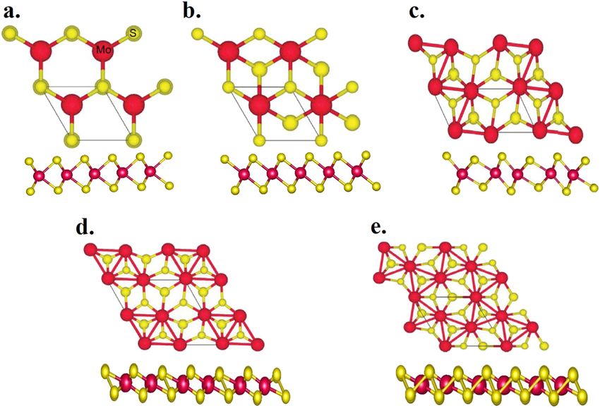
APL Materials                                                                                                   PERSPECTIVE                   scitation.org/journal/apm

                                                                                                                      √   √
      FIG. 1. Top and side views of (a) H, (b) T, (c) (1 × 2) supershell, T′ , (d) (2 × 2) supershell, T′′ , and (e) ( 3 × 3) supershell, T′′′ phases of MoS2 . The short Mo–Mo bonds
      are shown in red for panels (c)–(e). Reproduced with permission from Pal et al., Phys. Rev. B 96, 195426 (2017). Copyright 2017 APS.

    √         √
       3a0 × 3a0 with a trimerized clustering (T′′′ ) in Fig. 1(e).12,13                        dynamically unstable as phonon dispersion of this phase shows
    Such diverse polymorphic forms are of great importance, since their                         instability at the zone boundary.38 Despite such distinct properties
    electronic properties vary greatly, with the metastable T′ , T′′ , and                      expected of each variant, most of the experimental papers dealing
    T′′′ phases being semiconductors with varying bandgaps and the T                            with such chemically treated samples do not clearly identify the spe-
    phase being metallic. Because of this tuneability of electronic prop-                       cific phase formed, often using the term T or in few cases T′ in a
    erties, ranging from wide gap insulator to metal, MoS2 has emerged                          generic manner to denote a metastable phase. There are also several
    as a potential candidate for an extraordinarily diverse range of novel                      reports where, instead of identifying any crystallographic phase, the
    applications in different fields, such as transistors,14,15 optoelectron-                   additional phases formed due to such chemical treatments are classi-
    ics,16 catalysis,2,17–19 photodetectors,20 supercapacitors,21 secondary                     fied by their presumed electronic or transport properties and termed
    batteries,22,23 and even superconductors.24,25                                              metallic or semiconducting MoS2 .33,41–43 Unfortunately, the generic
          MoS2 can be easily transformed into its various metastable                            use of T to denote the metastable form and the frequent claim of a
    states using different routes. These have been extensively studied and                      metallic nature have created an impression in the community that
    reported in the literature, such as plasma hot electron transfer,26,27                      the metastable state formed is predominantly the metallic, undis-
    mechanical strain,28,29 and electron-beam irradiation.30,31 However,                        torted T phase and not one of the small bandgap semiconducting,
    the chemical routes to achieve such transformation have proven to                           distorted T′ , T′′ , or T′′′ phases. We critically scrutinize this dogma
    be the most facile and, therefore, popular ones. Chemical routes,                           by looking at all relevant data already available in the literature to
    in turn, involve chemical,32,33 electrochemical alkali metal inter-                         arrive at the contrarian view in this perspective.
    calation34,35 or expansion of the interlayer distance by hydrother-
    mal synthesis.36,37 Although, through all the above-mentioned pro-
    cesses, the stable H phase is known to be transformed into one of
                                                                                                CHEMICAL EXFOLIATION OF MoS2
    the metastable states, the structure and electronic properties of the
    resultant phase have still remained highly contentious with many                                  Briefly, there are three distinct chemical exfoliation routes
    conflicting claims and ambiguities. Theoretical calculations pre-                           employed for MoS2 , namely, chemical intercalation, electrochemi-
    dict that the Jahn–Teller distorted T′ and T′′ are small bandgap                            cal intercalation, and hydrothermal or closely related solvothermal
    semiconductors38,39 and T′′′ is a ferroelectric insulator.40 Inter-                         synthesis. Schematic representations of these two routes are shown
    estingly, the undistorted T phase is theoretically predicted to be                          in Fig. 2. Historically, intercalation has been applied to layered

APL Mater. 8, 040909 (2020); doi: 10.1063/5.0005413                                                                                                                        8, 040909-2
© Author(s) 2020
APL Materials                                                                                            PERSPECTIVE             scitation.org/journal/apm

                                                      FIG. 2. Schematics of different chemical exfoliation techniques.

    materials as a means of exfoliating individual 2D layers from their                  with water.51 For the solvated phases of these types of compounds,
    bulk counterparts in large quantities. Intercalation chemistry plays a               the alkali metals remain almost fully ionized, and the guest (alkali
    key role in a majority of the liquid-based exfoliation methods, which,               atoms) and host charges (residual negative charges on disulfide lay-
    in contrast to the mechanical exfoliation, presents great advan-                     ers) remain separated by solvent layers. In the solvated phase, the
    tages for the mass production of 2D materials.44,45 The key princi-                  expansion of interlayer spacing with respect to that of the pris-
    ple for the intercalation-based exfoliation is to increase the inter-                tine compound naturally depends on the number of solvent layers
    layer spacing between individual layers by inserting foreign species.                formed in the interlayer space, which, in turn, depends on the ionic
    This weakens further the already weak interlayer van der Waals                       radius of the intercalated alkali metal. Thus, the distance between
    interaction and reduces the energy barrier of exfoliation.44                         the adjacent layers changes in a stepwise manner, depending on
          Although some research on the intercalation of different alkali                whether the solvating molecules form a monolayer or bilayer, as
    metals into MoS2 has been reported,46–49 most of the attention has                   demonstrated in Fig. 3(b).51,52 The hydration energy, characterized
    been focused on the intercalation of lithium (Li). This is based on                  by the charge/radius ratio, of Li+ and Na+ is higher due to the smaller
    the expectation that Li+ ions, with the smallest ionic radius among                  radius compared to the other alkali metal ions, leading to the for-
    all alkali metal ions, will easily enter the interlayer space and also               mation of two water layers in the intercalation compound for these
    because of the potential of such Li-intercalated materials as com-                   two guest ions, whereas all the other cations stabilize with mono-
    ponents of high-power rechargeable batteries. The chemical route                     layered packing of water in the interlayer space. While we focus
    of Li-intercalation, developed by Joensen and co-workers, involves                   our discussion primarily on the Li intercalation route in this arti-
    treating MoS2 with n-butyl lithium (n-BuLi) in hexane as the inter-                  cle, in view of its pre-eminence in the published literature as the
    calating agent, followed by a water exfoliation step.50 The schematic                most preferred route, we note in passing many other investigations
    illustration of the procedure is shown in Fig. 3(a). The key step                    of chemical intercalation driven exfoliation of MoS2 , involving other
    of this procedure is the formation of Lix MoS2 via a slow pro-                       alkali ions.49,53,54
    cess, requiring Li-intercalation about 48 h or more. The lithiated                         Electrochemical intercalation allows a considerably higher con-
    solid product is retrieved by filtration and washed with hexane to                   trol on the amount of Li-intercalated while also achieving a faster
    remove excess Li and organic residues of n-BuLi. In the next step of                 rate of intercalation for small quantities of the host, compared to
    washing with water, the bare alkali ions are immediately solvated                    the chemical intercalation route. In general, the Li+ electrochemical
    by water molecules that form a number of layers in the van der                       intercalation [see Fig. 3(c)] is performed in a test cell using a Li foil as
    Waals gap, facilitating the exfoliation process and also stabilizing the             the anode, LiPF6 or LiClO4 in propylene carbonate as the electrolyte,
    monolayers in the solvent.                                                           and MoS2 as the cathode using galvanostatic discharge at a certain
          However, for the solvated phase, the Li content is signifi-                    current density.55 The advantage of this method is that Li+ insertion
    cantly lower than in the intercalated compounds prior to washing                     can be monitored and precisely controlled so that the galvanostatic

APL Mater. 8, 040909 (2020); doi: 10.1063/5.0005413                                                                                                        8, 040909-3
© Author(s) 2020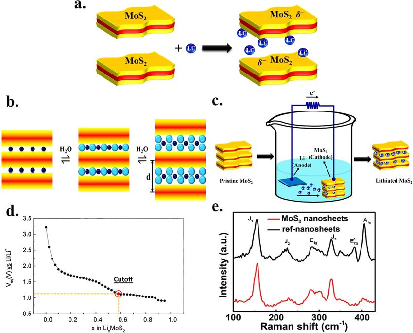
APL Materials                                                                                                   PERSPECTIVE                   scitation.org/journal/apm

      FIG. 3. (a) Schematics of lithium ion intercalation into the MoS2 matrix, (b) representation of the intercalated alkali metal cation with water molecules arranged in monolayer
      and bilayer, (c) schematics of the electrochemical intercalation method, and (d) voltage–composition curve for the intercalation of lithium into MoS2 to form Lix MoS2 . Cutoff
      voltage is shown with the red dot beyond which Lix MoS2 decomposes forming Li2 S. (e) Pure T′ phase of MoS2 prepared through the formation of Lix MoS2 via high temperature
      solid state synthesis followed by water exfoliation. Panel (d) is reproduced with permission from Benavente et al., Coord. Chem. Rev. 224, 87 (2002). Copyright 2002 Elsevier,
      and (e) is reproduced with permission from Guo et al., J. Mater. Chem. C 5, 5977 (2017). Copyright 2017 RSC.

    discharge can be stopped at the desired Li content to avoid decom-                          VIBRATIONAL STRUCTURE OF DIFFERENT PHASES
    position of the Li-intercalated compounds by optimizing the cutoff
                                                                                                     Raman spectroscopy has been used routinely in the literature
    voltage. Figure 3(d) shows a typical voltage–composition curve for
                                                                                                to differentiate different polymorphs of MoS2 , as it provides a reli-
    the intercalation of Li in H–MoS2 with the cutoff voltage shown with
                                                                                                able methodology based on the distinctive vibrational structures
    the red dot.56
                                                                                                expected from each phase. Any spectroscopic, including Raman,
         Hydrothermal57 and solvothermal58,59 syntheses are the two
                                                                                                transition probability is proportional to the square of the corre-
    other, closely interrelated, popular methods for chemical exfoliation
                                                                                                sponding transition matrix element given by
    of MoS2 by forcing small molecules into the interlayer gap, leading
    to the weakening of the van der Waals interaction between two adja-
    cent layers. Typically, in this method, molybdate is used to react with                                                      Ofi = ⟨ψf |Ô|ψi ⟩,                              (1)
    a sulfide or sulfur in a stainless-steel autoclave in the presence of
    a reducing agent, leading to a series of physicochemical reactions                          where ψ i and ψ f are the wavefunctions of the initial and final
    under a relatively high temperature (∼200 ○ C) and high pressure                            states of the transition and Ô is the transition operator. For an
    for several hours. In most of the cases, the resultant MoS2 with                            allowed transition, the integral in Eq. (1) has to be non-zero, which
    greater interlayer spacing is intercalated with NH4 + 36,60 or H2 O43                       can be simply translated in group theoretical terms by mentioning
    molecules.                                                                                  that for an allowed transition, the direct product of the irreducible

APL Mater. 8, 040909 (2020); doi: 10.1063/5.0005413                                                                                                                        8, 040909-4
© Author(s) 2020
APL Materials                                                                                              PERSPECTIVE                  scitation.org/journal/apm

    representation of the corresponding terms in Eq. (1) has to con-                       strains generated across the two phase boundaries, and possibili-
    tain a function that forms a basis for the totally symmetric irre-                     ties of charge doping, making the real scenario very different from
    ducible representation. In other words, Γf ⊗ ΓO ⊗ Γi must contain                      the idealized case considered by theoretical approaches; and many
    the totally symmetric irreducible representation for the transition                    of these additional effects may have the ability to make the finite-
    matrix element to be nonzero. The vibrational ground state ⟨ψi ∣ of                    sized and embedded and/or charge-doped T phase a metastable
    a molecule, relevant for Raman transitions, always transforms as the                   phase rather than an unstable phase under the experimental
    totally symmetric irreducible representation; therefore, the above                     realization.
    general condition, in the context of Raman spectroscopy, requires                            The above discussion on the maximum number of Raman
    that the direct product of Γf ⊗ ΓO has to contain a totally sym-                       peaks expected in any given phase of MoS2 is already a power-
    metric irreducible representation. For Raman spectroscopy, Ô is the                   ful tool to probe the possible phases formed. This is further aided
    polarizability operator. The irreducible representation (Γvib ), corre-                by detailed quantum mechanical calculations of the phonon spec-
    sponding to the normal modes of vibrations at the zone center (k                       trum of each phase, providing quantitative estimates of the various
    = 0) of the point group D3h describing the structure of monolayer                      peak positions. For example, in Table I, we have tabulated the the-
    MoS2 in its H phase,61 is given by                                                     oretically calculated frequencies for the three Raman active modes,
                                                                                                           1
                                                                                           namely, E1g , E2g  , and A1g in the H phase of MoS2 from Refs. 12,
                          Γvib (H) = A′1 + 2E′ + 2A′′2 + E′′ .                    (2)      38, and 63. We have also shown the experimentally obtained esti-
                                                                                           mates of the Raman peak positions for the H phase. The remarkable
    Careful inspection of the basis functions of each irreducible repre-                   agreement between the experiment and calculated values provides us
    sentation of the D3h point group reveals that A′1 , E′′ , and one of E′                with confidence in determining the specific phases of MoS2 present
    are the Raman active modes, which give rise to three peaks in the                      in any given sample of MoS2 from a scrutiny of its Raman spec-
    Raman spectra of this phase.                                                           trum. With this aim in mind, we have collected every publication
         By carrying out similar analysis on T (D3d point group) and T′                    on chemically exfoliated MoS2 that also reports the corresponding
    (C2h point group) phases, one immediately finds out that the irre-                     Raman spectrum. We summarize the comprehensive information
    ducible representations of the normal modes of vibrations are61,62                     available in the literature by tabulating the peak positions of the
                                                                                           Raman spectrum in each such publication together with the assign-
                         Γvib (T) = A1g + Eg + 2Eu + 2A2u ,                       (3)      ment of the nature of the metastable phase of MoS2 , suggested
                                                                                           in that publication in Table II. The top three rows of this table
                        Γvib (T′ ) = 6Ag + 3Bg + 3Au + 6Bu ,                      (4)      provide the summary of all theoretically calculated peak positions,
                                                                                           reported for various polymorphs of MoS2 so far in the literature,
    with the Raman active modes as A1g , Eg for the T phase (2 peaks)                      and we use these values for our own phase identifications of the
    and Ag , Bg (9 peaks) for the T′ phase. We note that this analysis                     reported spectra in the last column of this table. When we write
    does not provide any indication of how intense or weak a specific                      T′ + H in the last column, we imply that the most intense signal
    symmetry-allowed Raman signal may be; therefore, it is entirely pos-                   of the Raman spectrum reported in that reference arises from the
    sible that a symmetry-allowed Raman signal is not observed in an                       T′ phase, while there are also lower intensity signals present that
    experiment due to its low intensity. In this sense, the above con-                     are due to the presence of the H phase; H + T′ implies exactly the
    sideration helps to establish a rigorous upper limit on the num-                       opposite scenario. We have arranged the references in the chrono-
    ber of peaks one may observe for a given phase of MoS2 and not                         logical order and grouped them under the year of publication. For
    the lower limit. Before turning to the available information on the                    a quicker comprehension of all these disparate datasets in Table II,
    Raman spectra of these samples in the literature, we note the rea-                     we have represented these results also in the form of a plot in Fig. 4.
    son to consider the undistorted T phase as a possible candidate                        Table II and Fig. 4 together make evident a few interesting obser-
    despite the undeniable theoretical result that this is an unstable phase               vations. First, it appears that the claim of the T phase formation
    that will spontaneously distort itself into one of the lower energy                    was relatively more abundant until about 2017, while the claim
    T′ , T′′ , or T′′′ phases; in other words, theoretical analysis shows                  of the formation of the T′ phase has become relatively more fre-
    that it is purely unstable and cannot be a metastable state. How-                      quent in recent years. We also note that most of the Raman spectra
    ever, such theoretical analysis bases itself on the long-range periodic                reported in the literature invariably exhibit the signatures of the
    structure of the T phase, whereas the observed metastable states of                    H phase with peaks appearing at ∼382 cm−1 and ∼405 cm−1 . This
    MoS2 coexist as small patches within the domains of the H phase;                       suggests that the conversion of bulk MoS2 to its few layered 2D
    this leads to several additional effects, such as the finite size effect,              form via chemical exfoliation generally does not lead to a complete

                            TABLE I. Theoretically calculated and experimentally obtained peak position (in cm−1 ) in the Raman spectra of MoS2 in its
                            H phase.

                            H                                         First (E′′ /E1g )               Second (E′ /E12g )         Third (A′ 1 /A1g )

                            Theoretical calculation                  280–28612,63                      375–38512,38,63            402–40812,38,63
                            Experimental value                286 (very low intensity)61,64            380–38361,64–67            402–40961,64–67

APL Mater. 8, 040909 (2020); doi: 10.1063/5.0005413                                                                                                             8, 040909-5
© Author(s) 2020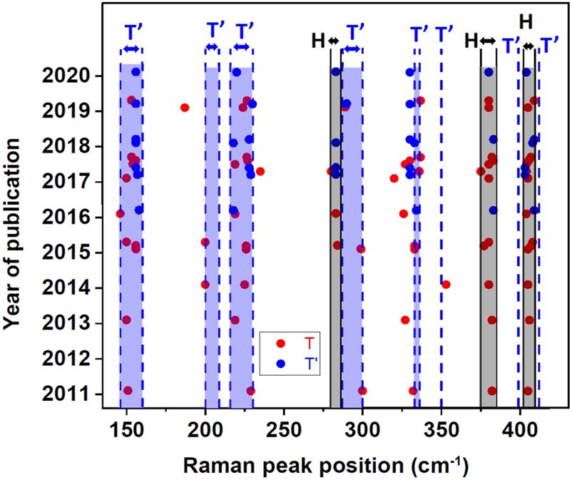
© Author(s) 2020
TABLE II. Theoretically calculated and experimentally obtained peak position (in cm-1 ) in the Raman spectra available in the literature for MoS2 in its different polymorphic phases. The first group of data are
from theoretical calculations for pure H, T and T′ phases, as indicated, and serve as reference values. Subsequent entries are for experimentally obtained Raman peak positions along with the claimed phases
in corresponding references with our assignments appearing in the last column under “Phase”. In case of a mixture of phases, the dominant one appears first. The publication years are shown in bold within
APL Materials
parentheses for the subsequent group of reports.
Reference Peak positions (cm−1 ) Claim Phase
12, 38, 61, 68,
280–286 375–385 402–409 H
and 69
12, 61, and 69 258–268 356–391 T
12, 38, 61,
APL Mater. 8, 040909 (2020); doi: 10.1063/5.0005413
138–140 146–160 200–209 216–230 286–300 333–336 350 399 412 T′
and 69–71
(2011)
33 151 229 300 332 382 405 T+H H + T′
(2013)
42 150 219 327 382 406 T+H H + T′
(2014)
72 200 225 353 380 405 T H + T′
(2015)
73 156 226 299 333 405 T+H T′ + H
60 156 226 284 333 377 407 T+H T′ + H
34 150 200 380 408 T+H T′ + H
(2016)
43 146 219 283 326 404 Metallic T′ + H
PERSPECTIVE
67 158 218 334 383 409 T′ + H T′ + H
(2017)
59 150 320 380 405 T+H T′ + H
74 157 229 283 330 403 T′ T′ + H
37 235 280 336 375 404 T+H T′ + H
25 156 228 283 330 403 T′ + H T′ + H
48 154 219 327 380 404 T+H T′ + H
32 156 227 330 383 405.4 T+H T′ + H
36 153.2 226.4 336.7 381.9 406.9 T+H T′ + H
scitation.org/journal/apm
8, 040909-6
© Author(s) 2020
                                                                                                                                                                            APL Materials

                   APL Mater. 8, 040909 (2020); doi: 10.1063/5.0005413
                                                                         TABLE II. (Continued.)

                                                                         Reference                                Peak positions (cm−1 )                 Claim    Phase

                                                                                                                               (2018)

                                                                         65                       156     218     283         333                 408    T′ + H   T′ + H
                                                                         62                       156     228                 330          383    409    T′ + H   T′ + H

                                                                                                                               (2019)

                                                                         75                        187     224    289                      380    405    T+H      T′ + H
                                                                         76                        156    ∼230    ∼290       ∼330                        T′ + H   T′ + H
                                                                         77                       153.2   226.5              336.8         ∼380   ∼409   T+H      T′ + H

                                                                                                                               (2020)

                                                                         78                       156     220     283         330          380    404    T′ + H   T′ + H
                                                                                                                                                                                PERSPECTIVE
                                                                                                                                                                           scitation.org/journal/apm

                   8, 040909-7
APL Materials PERSPECTIVE scitation.org/journal/apm
ELECTRONIC STRUCTURE CONSIDERATIONS
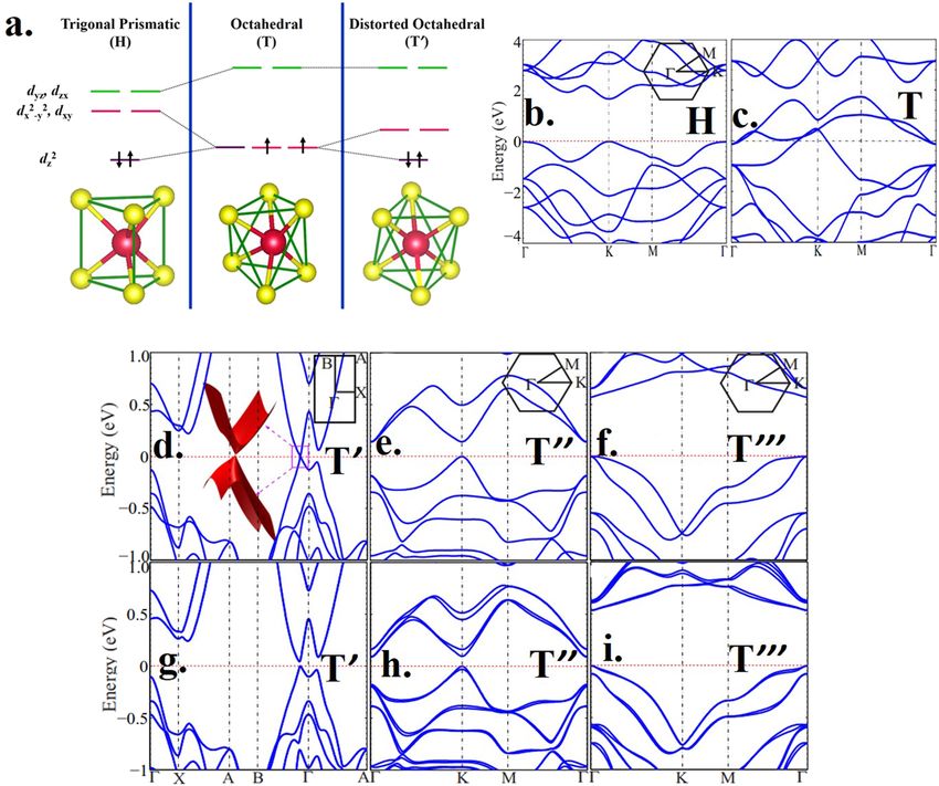
Electronic structures of different polymorphs of MoS2 can be
rationalized to a large extent in terms of their crystal structures based
on the ligand field theory. As shown in Fig. 5(a), the trigonal pris-
matic coordination of H phase MoS2 splits the five d-orbitals of Mo
into three groups of energies with the dz 2 orbital as the lowest energy
and separated from the remaining four orbitals by a large energy gap.
The two d-electrons of Mo in MoS2 occupy this lowest energy of the
dz 2 orbital making it filled and separated by a large gap from the two
sets of empty degenerate levels, namely, dx 2 −y 2 , dxy and dyz , dzx . In
contrast, the octahedral ligand field splitting in the case of the undis-
torted T phase leads to the splitting of the five d-orbitals into lower
energy, triply degenerate t 2g levels, separated by a large energy gap
from the doubly degenerate eg levels. In this case, the two d-electrons
of Mo, occupying the triply degenerate t 2g levels will give rise to par-
FIG. 4. A graphical representation of the results of all Raman studies available tially occupied states, implying a metallic nature of the system. How-
in the literature and tabulated in Table II. The peak positions of all Raman sig- ever, the ground state of the t 2g 3 electronic configuration is triply
nals reported in any given publication appear along a horizontal line, sorted by
the year of publication. The peak positions are represented with red symbols, if degenerate and is, therefore, unstable toward Jahn–Teller distor-
the authors attributed the dominant metastable state formed to the undistorted tions. Such distortions will split the triply degenerate t 2g orbitals into
T phase, while the blue symbols are used to designate those reports where the a lower lying doubly degenerate orbital group and a higher energy
authors attribute the dominant metastable phase to be T′ phase. Clearly, there singly degenerate orbital, as shown in the third panel of Fig. 5(a).
is a very good consistency in the peak positions between different reports, inde- One may then anticipate the formation of a semiconductor with a
pendent of the claim concerning the phase type, T or T′ . We have also marked
by vertical lines ranges of frequencies calculated for the H phase (in black) and
small bandgap, controlled by the Jahn–Teller distortions, in such
for the T′ phase (in blue). This makes it evident that all peak positions in chemi- a distorted phase, compared to the bandgap in the H phase deter-
cally exfoliated samples correspond to either the stable H phase or the distorted mined by the large ligand field splitting. Depending on the specific
T′ phase. distortions of the T phase, lifting the degeneracy of the ground state,
one arrives at the various semiconducting T′ , T′′ , and T′′′ phases
with small bandgaps. While this simplified molecular orbital (MO)
diagram provides one with a qualitative expectation of the differing
transformation of the stable H phase to its various metastable T electronic structures for the various crystallographic polymorphs of
forms. Most importantly, we find that all Raman spectra published MoS2 , the actual magnitudes of the bandgaps will be determined by
so far to provide evidence of metastable states in chemically exfoli- the extensive dispersion of the local molecular orbitals in the peri-
ated, few layer MoS2 have three or more Raman peaks in addition odic solid forming bands. This can even induce qualitative changes
to those attributable to the presence of H phase in the sample. One in the metallic/insulating properties if the dispersional widths of the
notable exception is achieved via a high temperature solid state syn- relevant bands become comparable to or larger than the gaps in the
thesis of Lix MoS2 and successive exfoliation in aqueous acidic solu- MO energy level diagrams shown schematically in Fig. 5(a). Band
tion, leading to the formation of the homogeneous T′ phase instead structures have been calculated by many groups for various poly-
of the mixtures of H, T, and T′ phases.74 The Raman spectra of this morphic forms of MoS2 using a variety of approximations based on
sample are compared with those of a sample synthesized through the different first principles approaches. Such calculations find that the
traditional intercalation route using n-BuLi in Fig. 3(e). The com- H form of MoS2 is indeed the lowest energy phase and the T form
1
plete absence of the E2g mode (383 cm−1 ), characteristic of the H constitutes an unstable phase, undergoing spontaneous distortions
phase, establishes the absence of any H phase in this sample, while to T′ , T′′ , and T′′′ structures, in broad agreement with the arguments
the signal due to the E2g 1 mode is clearly visible in the n-BuLi treated presented above based on Fig. 5(a).12,38,39,69 The calculated bandgap
sample mentioned as ref-nanosheets in Fig. 3(e). The clear obser- of the H phase of MoS2 shows both quantitative and qualitative
vation of more than two peaks from the metastable phase in every dependencies on the number of layers of MoS2 involved with the
reported case of Raman spectra, as shown in Table II, establishes bandgap varying from nearly 1.2 eV for the bulk to about 1.8 eV in
the absence of any significant extent of the undistorted, metallic T the monolayer form; moreover, the nature of the bandgap is a direct
phase formation in the chemical exfoliation route; this is not entirely one for the single layer, while multilayer H MoS2 presents an indirect
surprising in view of the intrinsic instability of the T phase. What bandgap82,83 with ample experimental validations84,85 of these sug-
is surprising, however, is the often reported79–81 metallic nature of gestions. Figure 5(b), showing the band dispersions for a single layer
the chemically exfoliated MoS2 samples, since the H phase and all of H–MoS2 , exhibits the direct bandgap of 1.67 eV,39 at the k points,
metastable distorted phases, such as T′ , T′′ , and T′′′ , are known to be consistent with other calculations.13,86 The calculated band disper-
semiconducting. Since the question of metallic/insulating behavior sions for a monolayer of the unstable T-MoS2 show three bands
of any sample is intrinsically connected with its electronic struc- crossing the Fermi level, confirming its metallic nature, as illustrated
ture, next, we turn to the discussion of electronic structures of such in Fig. 5(c). The band structures of monolayers of distorted octahe-
samples. dral phases (T′ , T′′ , and T′′′ ) of MoS2 are shown in Figs. 5(d)–5(e).
APL Mater. 8, 040909 (2020); doi: 10.1063/5.0005413 8, 040909-8
© Author(s) 2020APL Materials PERSPECTIVE scitation.org/journal/apm
FIG. 5. (a) The building [MoS6 ] unit of the H, T′ , and T phase with the corresponding 4d orbital splitting of central Mo+4 ; Calculated electronic band structures of the monolayer
of (b) H phase, (c) T phase, and different distorted octahedral phases, i.e., (d) T′ , (e) T′′ , and (f) T′′′ . The corresponding band structures with SOC are shown in the lower
panel for (g) T′ , (h) T′′ , and (i) T′′′ . Panels (b)–(i) are reproduced with permission from Zhuang et al., Phys. Rev. B 96, 165305 (2017). Copyright 2017 APS.
From these figures, it is evident that both T′′ and T′′′ phases have origin and the nature of unusual properties of chemically exfoliated
bandgaps [see Figs. 5(e) and 5(f)] of about 14 meV and 57 meV, sig- 2D MoS2 revolve around the primary issues: what is the most abun-
nificantly smaller than that in the H phase [Fig. 5(b)]. The T′ appears dant additional phase formed, T or T′ ; and what is the electronic
to have a Dirac cone formed between B and Γ points, as illustrated in properties of that state? Is it metallic or semiconducting? Theoretical
Fig. 5(d). However, it has been shown by some authors that incorpo- considerations, of course, suggest that the T phase in the extended
rating spin–orbit coupling (SOC) within the Mo 4d in the calculation bulk form is not even a metastable state, but a dynamically unstable
leads to the splitting of this Dirac cone and opening of a bandgap of state;38,40 in addition, the formation energy of the T phase is quite
∼50 meV [Fig. 5(g)].39 There are other reports suggesting the for- high compared to that of the T′ phase,39 making the formation of
mation of a similarly small bandgap (≤100 meV) for the T′ phase by the T phase in preference over the T′ phase unlikely. As already
several groups.32,87 Since some of these calculations do not involve shown in Table II, several claims of the formation of the T phase
SOC, the essential role of SOC in forming the bandgap in the T′ were based on additional Raman peaks appearing in the spectra of
phase is not fully established. SOC decreases the bandgap of the T′′ the exfoliated samples. Many of these publications interpret the T
structure, while the bandgap of the T′′′ structure is almost unaffected phase formation erroneously citing the original works in Refs. 61
by the SOC, as shown in Figs. 5(h) and 5(i), respectively. and 70, since these original publications already referred to the for-
We now focus on experimental investigations leading to claims mation of the (2 × 1) distorted T phase, which in today’s terminology
of formation of specific polymorphs, other than the stable H phase, is the T′ phase. Since we have discussed the Raman results earlier
due to the chemical exfoliations of MoS2 in the 2D forms. Apart from in this article, we focus our attention to other experimental probes
T and T′ , mention of other metastable phases, such as T′′ and T′′′ , into the nature of the metastable states formed. While the erroneous
is almost non-existent in the experimental literature. Therefore, the conclusion of the T phase formation based on Raman studies led
APL Mater. 8, 040909 (2020); doi: 10.1063/5.0005413 8, 040909-9
© Author(s) 2020APL Materials PERSPECTIVE scitation.org/journal/apm
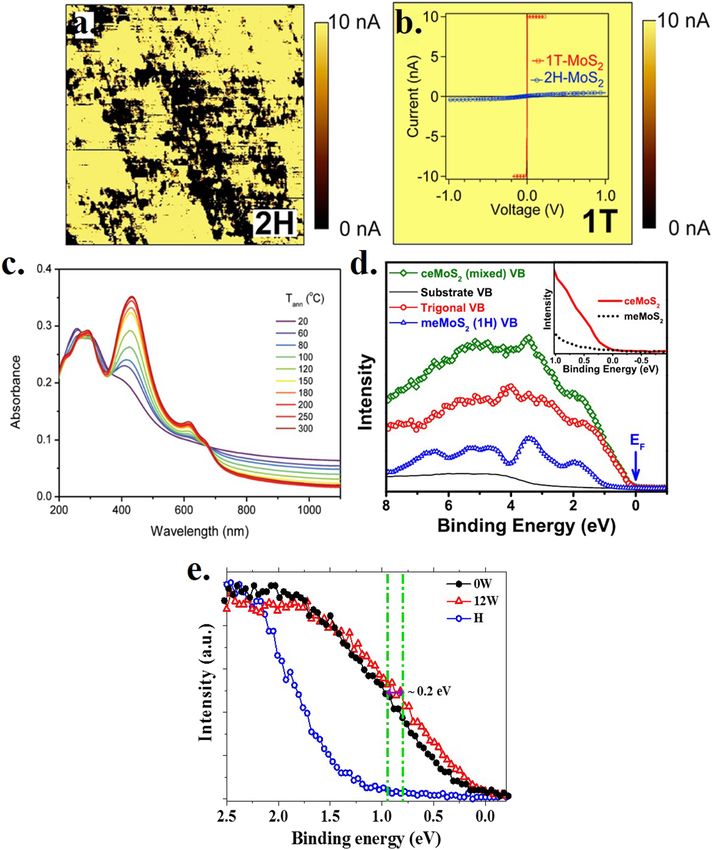
many groups to conclude, consequently, a metallic nature, there are (CSAFM) on MoS2 before and after the chemical exfoliation are
also reports of some direct investigations of the electronic structure shown in Figs. 6(a) and 6(b) in terms of the representative con-
and transport properties that are relevant in the present context. ductivity maps.42 Curiously, the conductivity map of the pristine H
For example, the results of current sensing atomic force microscopy sample in Fig. 6(a) exhibits extreme inhomogeneity, with patches of
FIG. 6. Conductivity maps of (a) pristine MoS2 and (b) chemically exfoliated MoS2 . Superimposed on the conductivity map in (b) is the I–V plot of the corresponding samples.
(c) The absorption spectra of lithium intercalated and exfoliated MoS2 flakes at different annealing temperatures; (d) valence band spectra obtained from mechanically
(meMoS2 ) and chemically exfoliated (ceMoS2 ) samples along with the calculated valence band of the pure T′ phase, inset showing the zoomed-in view of the Fermi energy
edge for both the samples; and (e) spectra near the Fermi edges for pristine H and the samples with a different extent of Li+ present in it. Panels (a) and (b) are reproduced
with permission from Lukowski et al., J. Am. Chem. Soc. 135, 10274 (2013). Copyright 2013 ACS; (c) reproduced with permission from Eda et al., Nano Lett. 11, 5111 (2011).
Copyright 2011 ACS; (d) reproduced with permission from Pal et al., Phys. Rev. B 96, 195426 (2017). Copyright 2017 APS; and (e) Pariari et al., Appl. Mater. Today 19,
100544 (2020). Copyright 2020 Elsevier.
APL Mater. 8, 040909 (2020); doi: 10.1063/5.0005413 8, 040909-10
© Author(s) 2020APL Materials PERSPECTIVE scitation.org/journal/apm
highly insulating regions, marked black on a surprisingly conduct- exfoliated sample (ceMoS2 ), establishing the semiconducting nature
ing major phase on the surface of a well-known insulating H phase, of the metastable state, consistent with the interpretation of the for-
possibly arising from the limitations of the technique or the sam- mation of the T′ phase. The above interpretation, however, does
ple. On the other hand, more relevant to the present discussion, the not explain why several past experiments found evidence of sub-
map of the chemically exfoliated sample in Fig. 6(b) presents a highly stantial conductivity for such metastable states. One possibility, of
conducting homogeneous surface. The I–V diagram, also shown in course, is that the thermally excited charge carriers are substantial
Fig. 6(b), was used to assert the metallic nature of the chemically for such a small bandgap semiconductor, whereas such charge car-
exfoliated sample. In passing, we note that the I–V curve of the riers will be entirely negligible for the large bandgap H phase. In
exfoliated sample in Fig. 6(b) is unusual with a highly non-ohmic, addition, we need to consider the possibility of charge carrier dop-
switching behavior for an extremely small threshold voltage followed ing of such a small bandgap semiconductor as a plausible origin of
by current saturations, not expected of a usual metal. Despite these the observed conductivity. In order to address this possibility, we
unusual aspects, these experiments point to a reasonable conduc- prepared samples with a different extent of Li+ ions present in it
tivity of the chemically exfoliated sample. The absorbance data of by simply varying the water washing cycle after Li-intercalation.78
chemically exfoliated samples have also been used33 to suggest the The valence band spectra from the two extremes of washing, namely,
existence of the metallic T phase. Reference 33 has also reported no washing at all (termed 0W) and after 12 cycles of washing with
the systematic change in the optical absorbance spectra, accompa- water (12W), are shown in Fig. 6(e). These spectra with essentially
nying the conversion of the metastable phase to the stable one as zero intensity at the Fermi energy establish both samples as small
a function of the annealing temperature. These absorbance spectra bandgap semiconductors. We also find that the valence band spec-
are shown in Fig. 6(c). Spectral features, preferentially present in the trum obtained from the 12W sample is shifted toward the higher
sample with higher proportion of the large bandgap H phase follow- binding energy side by almost 0.2 eV, indicating electron doping of
ing the higher temperature annealing, are interpreted as excitonic MoS2 by the Li ions. Therefore, it is possible that such charge doping
features. It was argued that the absence of any excitonic peak in the of the chemically exfoliated MoS2 samples contributes to the con-
exfoliated sample at room temperature indicated that the as syn- duction though the polymorphic phase remains T′ , as suggested by
thesized, exfoliated sample was metallic and, consequently, existed the Raman frequencies and low photoelectron spectral intensity at
in the T polymorphic form. However, as pointed out in Table II, the EF .
the as-synthesized sample in this case exhibited J1 (151 cm−1 ), J2 In summary, we first discussed different routes to chemical
(229 cm−1 ), E1g (300 cm−1 ), and J3 (332 cm−1 ) peaks in its Raman exfoliation of bulk MoS2 that provide the most convenient ways to
spectrum, and this is inconsistent with high symmetry of the undis- synthesize copious amounts of 2D MoS2 . Such chemical exfoliation
torted T phase. In this context, we note that there is a significant has been shown to give rise to several polymorphs of MoS2 in addi-
level of absorbance, extending to the longest wavelength displayed tion to the most stable H phase, and many interesting properties and
in Fig. 6(c), for the chemically exfoliated sample without annealing. device applications of such samples have been attributed in the past
This featureless absorbance must be associated with the metastable literature to the presence of these additional phases. Surveying the
phase formed, since the absorbance is found to decrease systemat- existing literature, we help to focus on the ambiguities present in
ically with an increasing conversion of the metastable state to the identifying the dominant polymorphic phase in such samples and
stable H phase with a large bandgap (∼1.8 eV or ∼690 nm) with the show that the existing literature in terms of Raman spectra provides
successively higher annealing temperatures. This allows for the pos- overwhelming evidence in favor of the T′ phase being present, rather
sibility of a small bandgap existing for the metastable phase, since than the often stated T phase. Since the T′ phase is known to be
the excitonic peak for that phase will appear in the vicinity of its semiconducting, we then address the puzzling issue of several more
bandgap. Considering that the various estimates of the bandgap of direct probes of the electronic structures of these samples, which
the T′ phase are smaller than 100 meV, the spectral features in appears to point to a highly conducting state of such exfoliated sam-
Fig. 6(c) do not exclude the possibility of the metastable state being ples. We show that the substantial conductivity has to be understood
the T′ phase with its observable excitonic features lying outside of in terms of thermal and dopant induced charge-carrier dopings of
the wavelengths probed and presented in Fig. 6(c). the small bandgap T′ phase, rather than in terms of the formation of
It is well-known that the issue of metal/insulator property can the unstable, metallic T phase.
be most easily probed by photoelectron spectroscopy as it maps out
electron states directly. Thus, it characterizes a metal in the pres-
ence of a finite photoelectron spectral intensity at the Fermi energy, ACKNOWLEDGMENTS
while an insulator is characterized by a finite energy gap between The authors would like to thank SERB, Nanomission and DST,
the Fermi energy and the onset of the finite spectral intensity. In Government of India, and Jamsetji Tata Trust for the support of this
order to enhance the contribution from the metastable phase to research. D.P. acknowledges the Council of Scientific and Industrial
photoelectron spectra, we performed32 the scanning photoelectron Research for a student fellowship.
microscopy experiment with a photon beam size down to 120 nm.
The photon beam was positioned on the sample to maximize the
contribution of the metastable state, and the valence band spec- REFERENCES
tra were obtained from the same spot. A magnified view of the 1
K. S. Novoselov, A. K. Geim, S. V. Morozov, D. Jiang, Y. Zhang, S. V. Dubonos,
energy region around the Fermi energy is shown in the inset of I. V. Grigorieva, and A. A. Firsov, Science 306, 666 (2004).
2
Fig. 6(d). Clearly, the spectral intensity at the Fermi energy is negligi- W. Zhong, W. Tu, S. Feng, and A. Xu, J. Alloys Compd. 772, 669 (2019).
3
bly small for both the H phases, termed meMoS2 , and the chemically P. Afanasiev, J. Catal. 269, 269 (2010).
APL Mater. 8, 040909 (2020); doi: 10.1063/5.0005413 8, 040909-11
© Author(s) 2020APL Materials PERSPECTIVE scitation.org/journal/apm
4 39
E. Devers, P. Afanasiev, B. Jouguet, and M. Vrinat, Catal. Lett. 82, 13 (2002). H. L. Zhuang, M. D. Johannes, A. K. Singh, and R. G. Hennig, Phys. Rev. B 96,
5 165305 (2017).
G. Salomon, A. W. J. De Gee, and J. H. Zaat, Wear 7, 87 (1964).
6 40
M. R. Hilton, R. Bauer, S. V. Didziulis, M. T. Dugger, J. M. Keem, and J. Schol- S. N. Shirodkar and U. V. Waghmare, Phys. Rev. Lett. 112, 157601 (2014).
41
hamer, Surf. Coat. Technol. 53, 13 (1992). L. Li, J. Chen, K. Wu, C. Cao, S. Shi, and J. Cui, Nanomaterials 9, 1366 (2019).
7 42
M. Chhowalla and G. A. J. Amaratunga, Nature 407, 164 (2000). M. A. Lukowski, A. S. Daniel, F. Meng, A. Forticaux, L. Li, and S. Jin, J. Am.
8 Chem. Soc. 135, 10274 (2013).
I. Song, C. Park, and H. C. Choi, RSC Adv. 5, 7495 (2015).
9 43
R. G. Dickinson and L. Pauling, J. Am. Chem. Soc. 45, 1466 (1923). X. Geng, W. Sun, W. Wu, B. Chen, A. Al-Hilo, M. Benamara, H. Zhu, F. Watan-
10
T. Böker, R. Severin, A. Müller, C. Janowitz, R. Manzke, D. Voß, P. Krüger, abe, J. Cui, and T. P. Chen, Nat. Commun. 7, 10672 (2016).
44
A. Mazur, and J. Pollmann, Phys. Rev. B 64, 235305 (2001). V. Nicolosi, M. Chhowalla, M. G. Kanatzidis, M. S. Strano, and J. N. Coleman,
11
K. F. Mak, C. Lee, J. Hone, J. Shan, and T. F. Heinz, Phys. Rev. Lett. 105, 136805 Science 340, 1226419 (2013).
45
(2010). J. N. Coleman, M. Lotya, A. O’Neill, S. D. Bergin, P. J. King, U. Khan, K. Young,
12
T. Hu, R. Li, and J. Dong, J. Chem. Phys. 139, 174702 (2013). A. Gaucher, S. De, R. J. Smith, I. V. Shvets, S. K. Arora, G. Stanton, H.-Y. Kim,
13 K. Lee, G. T. Kim, G. S. Duesberg, T. Hallam, J. J. Boland, J. J. Wang, J. F. Donegan,
M. Kan, J. Y. Wang, X. W. Li, S. H. Zhang, Y. W. Li, Y. Kawazoe, Q. Sun, and
J. C. Grunlan, G. Moriarty, A. Shmeliov, R. J. Nicholls, J. M. Perkins,
P. Jena, J. Phys. Chem. C 118, 1515 (2014).
14 E. M. Grieveson, K. Theuwissen, D. W. McComb, P. D. Nellist, and V. Nicolosi,
B. Radisavljevic, A. Radenovic, J. Brivio, V. Giacometti, and A. Kis, Nat.
Science 331, 568 (2011).
Nanotechnol. 6, 147 (2011). 46
15 Y. Wang, J. Z. Ou, S. Balendhran, A. F. Chrimes, M. Mortazavi, D. D. Yao, M.
S. Ghatak, S. Mukherjee, M. Jain, D. D. Sarma, and A. Ghosh, APL Mater. 2,
R. Field, K. Latham, V. Bansal, J. R. Friend, S. Zhuiykov, N. V. Medhekar, M.
092515 (2014).
16
S. Strano, and K. Kalantar-Zadeh, ACS Nano 7, 10083 (2013).
Z. Yin, H. Li, H. Li, L. Jiang, Y. Shi, Y. Sun, G. Lu, Q. Zhang, X. Chen, and 47
G. Li, D. Luo, X. Wang, M. H. Seo, S. Hemmati, A. Yu, and Z. Chen, Adv. Funct.
H. Zhang, ACS Nano 6, 74 (2012).
17
Mater. 27, 1702562 (2017).
B. Hinnemann, P. G. Moses, J. Bonde, K. P. Jørgensen, J. H. Nielsen, S. Horch, 48
N. H. Attanayake, A. C. Thenuwara, A. Patra, Y. V. Aulin, T. M. Tran,
I. Chorkendorff, and J. K. Nørskov, J. Am. Chem. Soc. 127, 5308 (2005). H. Chakraborty, E. Borguet, M. L. Klein, J. P. Perdew, and D. R. Strongin, ACS
18
X.-Y. Yu, Y. Feng, Y. Jeon, B. Guan, X. W. D. Lou, and U. Paik, Adv. Mater. 28, Energy Lett. 3, 7 (2018).
9006 (2016). 49
V. Alexiev, H. Meyer Zu Altenschildesche, R. Prins, and T. Weber, Chem.
19
T. F. Jaramillo, K. P. Jorgensen, J. Bonde, J. H. Nielsen, S. Horch, and I. Chork- Mater. 11, 1742 (1999).
endorff, Science 317, 100 (2007). 50
P. Joensen, R. F. Frindt, and S. R. Morrison, Mater. Res. Bull. 21, 457
20
O. Lopez-Sanchez, D. Lembke, M. Kayci, A. Radenovic, and A. Kis, Nat. (1986).
Nanotechnol. 8, 497 (2013). 51
A. S. Golub, Y. V. Zubavichus, Y. L. Slovokhotov, and Y. N. Novikov, Russ.
21
D. Sarkar, D. Das, S. Das, A. Kumar, S. Patil, K. K. Nanda, D. D. Sarma, and Chem. Rev. 72, 123 (2003).
A. Shukla, ACS Energy Lett. 4, 1602 (2019). 52
M. Danot, J. L. Mansot, A. S. Golub, G. A. Protzenko, P. B. Fabritchnyi,
22
N. Imanishi, K. Kanamura, and Z. I. Takehara, J. Electrochem. Soc. 139, 2082 Y. N. Novikov, and J. Rouxel, Mater. Res. Bull. 29, 833 (1994).
(1992). 53
F. Wypych and R. Schöllhorn, J. Chem. Soc. Chem. Commun. 1992(19), 1386.
23
K. Chang and W. Chen, ACS Nano 5, 4720 (2011). 54
F. Wypych, T. Weber, and R. Prins, Surf. Sci. 380, L474 (1997).
24
D. Costanzo, S. Jo, H. Berger, and A. F. Morpurgo, Nat. Nanotechnol. 11, 339 55
Z. Zeng, T. Sun, J. Zhu, X. Huang, Z. Yin, G. Lu, Z. Fan, Q. Yan, H. H. Hng, and
(2016). H. Zhang, Angew. Chem., Int. Ed. 51, 9052 (2012).
25
C. Guo, J. Pan, H. Li, T. Lin, P. Liu, C. Song, D. Wang, G. Mu, X. Lai, H. Zhang, 56
E. Benavente, M. A. Santa Ana, F. Mendizábal, and G. González, Coord. Chem.
W. Zhou, M. Chen, and F. Huang, J. Mater. Chem. C 5, 10855 (2017). Rev. 224, 87 (2002).
26
Y. Kang, Y. Gong, Z. Hu, Z. Li, Z. Qiu, X. Zhu, P. M. Ajayan, and Z. Fang, 57
X. Zhou, B. Xu, Z. Lin, D. Shu, and L. Ma, J. Nanosci. Nanotechnol. 14, 7250
Nanoscale 7, 4482 (2015). (2014).
27 58
Y. Kang, S. Najmaei, Z. Liu, Y. Bao, Y. Wang, X. Zhu, N. J. Halas, P. Nordlander, X. Feng, Q. Tang, J. Zhou, J. Fang, P. Ding, L. Sun, and L. Shi, Cryst. Res.
P. M. Ajayan, J. Lou, and Z. Fang, Adv. Mater. 26, 6467 (2014). Technol. 48, 363 (2013).
28 59
Z. Ding, Q.-X. Pei, J.-W. Jiang, and Y.-W. Zhang, J. Phys. Chem. C 119, 16358 L. Huang, Q. Wei, X. Xu, C. Shi, X. Liu, L. Zhou, and L. Mai, Phys. Chem. Chem.
(2015). Phys. 19, 13696 (2017).
29 60
A. Castellanos-Gomez, R. Roldán, E. Cappelluti, M. Buscema, F. Guinea, Q. Liu, X. Li, Q. He, A. Khalil, D. Liu, T. Xiang, X. Wu, and L. Song, Small 11,
H. S. J. Van Der Zant, and G. A. Steele, Nano Lett. 13, 5361 (2013). 5556 (2015).
30 61
Y.-C. Lin, D. O. Dumcenco, Y.-S. Huang, and K. Suenaga, Nat. Nanotechnol. 9, S. Jiménez Sandoval, D. Yang, R. F. Frindt, and J. C. Irwin, Phys. Rev. B 44, 3955
391 (2014). (1991).
31 62
S. Kretschmer, H.-P. Komsa, P. Bøggild, and A. V. Krasheninnikov, J. Phys. S. J. R. Tan, S. Sarkar, X. Zhao, X. Luo, Y. Z. Luo, S. M. Poh, I. Abdelwahab,
Chem. Lett. 8, 3061 (2017). W. Zhou, T. Venkatesan, W. Chen, S. Y. Quek, and K. P. Loh, ACS Nano 12, 5051
32
B. Pal, A. Singh, G. Sharada, P. Mahale, A. Kumar, S. Thirupathaiah, H. Sezen, (2018).
63
M. Amati, L. Gregoratti, U. V. Waghmare, and D. D. Sarma, Phys. Rev. B 96, H. Terrones, E. Del Corro, S. Feng, J. M. Poumirol, D. Rhodes, D. Smirnov,
195426 (2017). N. R. Pradhan, Z. Lin, M. A. T. Nguyen, A. L. Elías, T. E. Mallouk, L. Balicas,
33
G. Eda, H. Yamaguchi, D. Voiry, T. Fujita, M. Chen, and M. Chhowalla, Nano M. A. Pimenta, and M. Terrones, Sci. Rep. 4, 4215 (2014).
64
Lett. 11, 5111 (2011). G. Zhu, J. Liu, Q. Zheng, R. Zhang, D. Li, D. Banerjee, and D. G. Cahill, Nat.
34
F. Xiong, H. Wang, X. Liu, J. Sun, M. Brongersma, E. Pop, and Y. Cui, Nano Commun. 7, 13211 (2016).
65
Lett. 15, 6777 (2015). Y. Yu, G.-H. Nam, Q. He, X.-J. Wu, K. Zhang, Z. Yang, J. Chen, Q. Ma, M. Zhao,
35
M. Azhagurajan, T. Kajita, T. Itoh, Y.-G. Kim, and K. Itaya, J. Am. Chem. Soc. Z. Liu, F.-R. Ran, X. Wang, H. Li, X. Huang, B. Li, Q. Xiong, Q. Zhang, Z. Liu,
138, 3355 (2016). L. Gu, Y. Du, W. Huang, and H. Zhang, Nat. Chem. 10, 638 (2018).
36 66
D. Wang, X. Zhang, S. Bao, Z. Zhang, H. Fei, and Z. Wu, J. Mater. Chem. A 5, C. Lee, H. Yan, L. E. Brus, T. F. Heinz, J. Hone, and S. Ryu, ACS Nano 4, 2695
2681 (2017). (2010).
37 67
Z. Liu, Z. Gao, Y. Liu, M. Xia, R. Wang, and N. Li, ACS Appl. Mater. Interfaces K. Leng, Z. Chen, X. Zhao, W. Tang, B. Tian, C. T. Nai, W. Zhou, and K. P. Loh,
9, 25291 (2017). ACS Nano 10, 9208 (2016).
38 68
M. Calandra, Phys. Rev. B 88, 245428 (2013). J. L. Verble and T. J. Wieting, Phys. Rev. Lett. 25, 362 (1970).
APL Mater. 8, 040909 (2020); doi: 10.1063/5.0005413 8, 040909-12
© Author(s) 2020APL Materials PERSPECTIVE scitation.org/journal/apm
69 78
A. Singh, S. N. Shirodkar, and U. V. Waghmare, 2D Mater. 2, 035013 (2015). D. Pariari, R. M. Varma, M. N. Nair, P. Zeller, M. Amati, L. Gregoratti, K.
70 K. Nanda, and D. D. Sarma, Appl. Mater. Today 19, 100544 (2020).
D. Yang, S. Jiménez Sandoval, W. M. R. Divigalpitiya, J. C. Irwin, and R.
79
F. Frindt, Phys. Rev. B 43, 12053 (1991). K. Pramoda, M. M. Ayyub, N. K. Singh, M. Chhetri, U. Gupta, A. Soni, and C.
71 N. R. Rao, J. Phys. Chem. C 122, 13376 (2018).
R. Saito, Y. Tatsumi, S. Huang, X. Ling, and M. S. Dresselhaus, J. Phys.: Condens.
80
Matter 28, 353002 (2016). P. Vishnoi, K. Pramoda, U. Gupta, M. Chhetri, R. G. Balakrishna, and C. N.
72 R. Rao, ACS Appl. Mater. Interfaces 11, 27780 (2019).
L. Guardia, J. I. Paredes, J. M. Munuera, S. Villar-Rodil, M. Ayán-Varela,
81
A. Martínez-Alonso, and J. M. D. Tascón, ACS Appl. Mater. Interfaces 6, 21702 U. Gupta and C. N. R. Rao, Nano Energy 41, 49 (2017).
82
(2014). W. S. Yun, S. W. Han, S. C. Hong, I. G. Kim, and J. D. Lee, Phys. Rev. B 85,
73
M. Acerce, D. Voiry, and M. Chhowalla, Nat. Nanotechnol. 10, 313 (2015). 033305 (2012).
74 83
C. Guo, H. Li, W. Zhao, J. Pan, T. Lin, J. Xu, M. Chen, and F. Huang, J. Mater. Z. Y. Zhu, Y. C. Cheng, and U. Schwingenschl, Phys. Rev. B 84, 153402
Chem. C 5, 5977 (2017). (2011).
75 84
E. Er, H.-L. Hou, A. Criado, J. Langer, M. Möller, N. Erk, L. M. Liz-Marzán, and W. Jin, P. Yeh, N. Zaki, D. Zhang, J. T. Sadowski, A. Al-mahboob, A. M. Van
M. Prato, Chem. Mater. 31, 5725 (2019). Der Zande, D. A. Chenet, J. I. Dadap, I. P. Herman, P. Sutter, J. Hone, and
76
H. K. Ng, A. Abutaha, D. Voiry, I. Verzhbitskiy, Y. Cai, G. Zhang, Y. Liu, J. Wu, R. M. Osgood, Phys. Rev. Lett. 111, 106801 (2013).
85
M. Chhowalla, G. Eda, and K. Hippalgaonkar, ACS Appl. Mater. Interfaces 11, A. Splendiani, L. Sun, Y. Zhang, T. Li, J. Kim, C.-Y. Chim, G. Galli, and F. Wang,
12184 (2019). Nano Lett. 10, 1271 (2010).
77 86
D. Sun, D. Huang, H. Wang, G.-L. Xu, X. Zhang, R. Zhang, Y. Tang, D. A. Ei- H. Shi, H. Pan, Y. W. Zhang, and B. I. Yakobson, Phys. Rev. B 87, 155304
hady, W. Alshitari, A. S. Al-bogamii, K. Amine, and M. Shao, Nano Energy 61, (2013).
87
361 (2019). P. Mahadevan and B. Sanyal, private communications (January 2020).
APL Mater. 8, 040909 (2020); doi: 10.1063/5.0005413 8, 040909-13
© Author(s) 2020You can also read