Other stencil applications - considerations for glue and pin-in-hole reflow innovators in chemical etching since 1970 - Tecan
←
→
Page content transcription
If your browser does not render page correctly, please read the page content below
other stencil
applications

considerations for glue and
pin-in-hole reflow

innovators in chemical etching since 1970
8.1 Glue
Epoxy glue is used as a surface mount adhesive (SMA) to attach and maintain surface mount devices (SMD) to
the PCB surface throughout placement and wave soldering. As such, thicker stencils which enable increased
adhesive deposits are required.

Since the development of single component epoxy technology for use as a SMA, the methods of application
themselves have evolved, driven by the requirements for increased assembly speed and improved process
repeatability.

Adhesive stencil printing utilises existing production technology and techniques to optimise the efficiency required
from a surface mount line, particularly relevant when densely populated assemblies are processed. Total print
times of less than 15 seconds are achievable.

8.1.1 Wave soldering

                  Direction of travel
PCB

                                                                                                     Molten solder wave

           Flux

                                                                     Figure 8.1 Wave soldering principle stages: flux,
                                                                     pre-heat and solder
                                         Pre Heaters

Figure 8.2 Wave soldering machine              Figure 8.3 Conveyorised        Figure 8.4 PCB entering solder wave
                                               board transport

8.1.2 Glue stencils

The stencil technology differs from that used to print solder paste, where the intention is to transfer the entire
contents of the aperture onto the PCB. When glue printing, however, good use is made of the adhesive’s ability to
remain as a partial retention in the apertures. This is based on the simple relationship of the surface area of the
deposit base (PCB contact area) relative to the aperture wall surface area.

2     Tecan other stencil applications                                                                   www.stencils.co.uk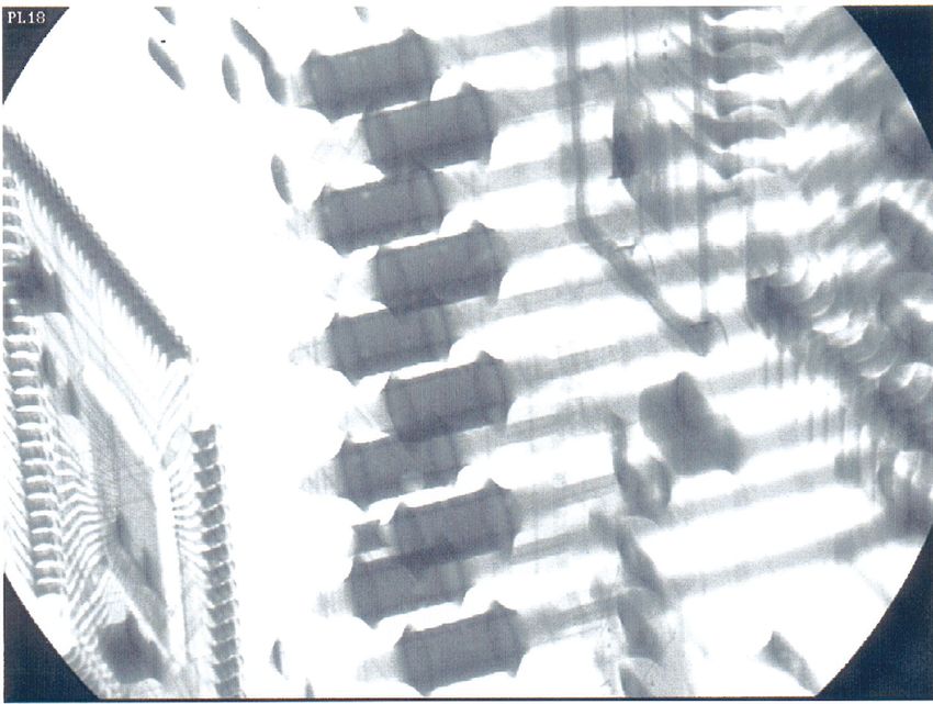
8.1.3 Glue printing principles

For components of a similar stand-off a stencil of 0.008” should be used. Where a variety of components exist
a stencil of 0.010” should be used. The resultant glue dot heights are a direct result of the aperture diameter
relative to the stencil thickness.

Where diameter = stencil thickness the dot heights are approx. 1/3 of the stencil thickness used. Using apertures
of twice the stencil thickness delivers dot heights of between one and two stencil thicknesses. Increasing the
aperture further delivers dots of approx. the stencil thickness.

Glue deposits can exist as single dots, double dots or simple slots. In each case it is important that the aperture
dimensions do not exceed 1/3 of the distance between the inner most edges of the discrete component pads.
The reason is that when a component is placed onto the adhesive dot it will flatten and spread out and the
contamination of the copper pads on the board with adhesive should be avoided at all cost.

Photo etched stencils can provide an aperture profile on the top of the stencil that assists with increased glue dot
heights. It is also possible using laser stencils to manufacture stencils with aperture sizes the same as the stencil
thickness, 0.200mm in 0.200mm (0.008” in 0.008”), this can be useful when the pads on the PCB are too close
together.

8.1.4 Multi height deposits

Where apertures are small, for example 0.012”/0.3mm, the adhesion between the glue and stencil effectively
retains some of the deposit and the resultant dots have a small or low Glue Dot Height (GDH).

Stencil apertures of 0.8mm (0.032”) ensure a larger percentage of the adhesive is transferred onto the PCB.
When the stencil and board are separated the stencil drags the adhesive and the resultant dots will be higher.

For apertures of between 0.060” to 0.080” (1.5mm to 2mm) most of the adhesive is transferred onto the PCB and
the GDH will be similar to the thickness of the stencil.

Each adhesive has individually distinct properties and characteristics which may require some process variations.
Most manufacturers offer guidelines and basic design rules to ensure compatibility with screen printing.

                                0.250mm (0.010”)    0.500mm (0.020”)            1.5mm (0.060”)

0.250mm (0.010”)

                                         1/3x            2x                         1x

Figure 8.5 Deposit height relative to glue dot diameter and stencil thickness

3     Tecan other stencil applications                                                                www.stencils.co.uk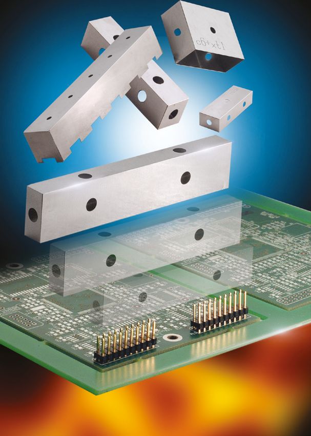
8.1.5 Glue stencil design

There are three variables to consider when designing the most effective pattern for SMD attachment:

•    Component standoff
•    Stencil thickness
•    Pad design

8.1.5.1 Component Standoff

                                                  This refers to the distance between the PCB and the underside of the
                                                  component, shown as x in figure 8.7 below.

                                                  Figure 8.6 Component standoff
                                                                                                           End terminations

A standoff of 0.002” (0.05mm) will cause
the deposit to spread 100% more than                                                                         Component

if it was 0.005” (0.125mm), see figure as                                                                          x

shown in figure 8.8.
                                                                                 PCB

                                                                                                           Component pads
                                                      Figure 8.7 Component standoff
                                                                                                                       d

                                    d

Adhesive deposit, after placement       Adhesive deposit, as printed (d / 3)   Adhesive deposit, after placement           Adhesive deposit, as printed (d / 3)

Figure 8.8 Effect of placement

The difference could be enough to allow the adhesive to spread onto the solder pads, causing joint contamination
and preventing effective soldering of the component. To avoid this problem, double dot printing is recommended
as shown in figure 8.9.

8.1.5.2 Stencil thickness

                                         Single dot
This is dependent upon the type of SMDs being   usedformat                     Double dot
                                                       but is usually between 0.008”      format(0.2-0.3mm). 0.008” Simple slot for
                                                                                      - 0.012”
(0.2mm) is more appropriate for components with similar standoffs and 0.010”-0.012” (0.25- 0.3mm) is used
where the mix of components require deposits of different heights (multi-height deposits).

4     Tecan other stencil applications                                                                                                       www.stencils.co.uk
8.1.5.3 Pad DesignAdhesive deposit, after placement          Adhesive deposit, as printed (d / 3)

This is usually dependent upon the clearance between the deposit and the component pads after placement.
Three alternatives are available as shown in figure 8.10

           Single dot format                      Double dot format                                 Simple slot format

8.1.6 GDD and GDH                                                                                       Figure 8.10 Dot formats

Glue dot diameter (GDD) and glue dot height (GDH) of the deposits depend on:

•    Diameter of stencil apertures
•    Stencil thickness selected
•    Viscosity/rheology of adhesive (manufacturer defined)
•    Surface roughness of the stencil (friction between adhesive and aperture walls)
•    PCB surface condition. An uncontaminated dry surface is necessary to ensure optimum adhesive printing

The following table shows approximate GDDs required when the adhesive has been printed with a metal
squeegee blade through a 0.010” (0.25mm) Tecan glue stencil.

    Component Size            GDD in mm   Component size      GDD in mm

    0402                      0.4         Mini-melf           1.1
    0603                      0.5         1812                1.4
    0805                      0.6         SO8                 3 x 1.5
    1206                      0.8         SO14                3 x 1.7
    SOT 23                    0.9

Equally good results have been achieved using multi-level stencils with 0.008” (0.200mm) general thickness rising
to 0.014” (0.350mm) in selected areas.

Tecan can create a glue stencil from the copper pad and silk screen data layers in combination with the
component designation file.

Some components have larger stand-offs and as such higher printed glue dots are required. It is crucial to
identify the components that need higher glue dots since too little glue will only result in loss of the components to
the solder wave.

Figure 8.11 Aperture modifications to increase GDH

5      Tecan other stencil applications                                                                         www.stencils.co.uk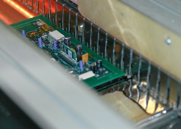
Aperture design and stencil thickness can be used to provide extra glue dot height.

The compass design enables the glue deposit to achieve a good solid base with the glue in the four points
contributing to glue dot height in the centre when the substrate separates from the stencil.

      Single dot                 Double dot              Simple dot             Compass

Figure 8.12 Aperture design

When higher glue dots are required to overcome increased component standoffs, use of the compass design may
need to be combined with both a normal print and a subsequent flood. Flooding is carried out without pressure
                                                                                        Print
and can leave a residue on the stencil that collapses into the larger apertures to provide an extruded dot height
of between three and five times the stencil thickness selected.

                                  Print                                                     Flood

Figure 8.13 Print and flood

8.1.7 Stencil cleaning

As the SMAs mentioned do not contain particulate matter, cleaning is easy and the selection of effective
stencil cleaning solutions will depend upon the stencil format, the SMA selected and the manufacturer’s
recommendations. Care must be taken when using mesh mounted stencils as some cleaning solutions,
                            Flood
concentrations and temperatures     required may attack or destroy the bonding agents.

          Aperture as                     Aperture not            Further ineffective
          purchased                       cleaned on              cleaning creates more
                                          1st attempt             build up similar to the
                                                                  annular rings on a tree

Figure 8.14 Stencil cleaning

6    Tecan other stencil applications                                                               www.stencils.co.uk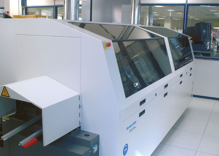
8.2 Pin-in-hole reflow (PIHR)
This assembly technique is used extensively as an alternative for
subsequent hand or wave soldering operations of leaded components
- from crystal oscillators and headers to multi-row connectors.

As with all surface mount technology, successful end product quality
relies on the accuracy and adequacy of the printed solder paste
deposits. Optimised stencil design is an essential requirement to
ensure the printing solution delivers successful PIHR results.

In its simplest form, the technique involves printing solder paste onto
the printed circuit board for both surface mount devices and leaded
components. With PIHR it is essential that sufficient paste volume is
available to ensure the required solder fillets are formed on the top
and bottom sides of the PCB and in the component holes.

Following insertion of leaded components and placement of surface
mount devices the assembly is reflowed. Shorter product cycle-times,
reductions in manufacturing costs and elimination of contamination
by second operation flux deposits are the main benefits.                         Figure 8.15 Pin-in-hole reflow (PIHR)

There are basic guidelines and considerations, which need to be followed to ensure success using this process.

8.2.1 PIHR criteria

8.2.1.1 Solder fillet appearance

Resultant PIHR solder fillets can have a flatter profile than those from hand or wave solder processes but with
careful paste volume matching it is possible to create fillets that resemble the traditionally accepted profiles. One
important consideration is that solder paste, although 88-92% metal by weight, is only approximately 50% by
volume. This cannot be ignored when calculating the theoretical solder fillet volume required, since absence of
paste volume before reflow will only lead to insufficient solder fillets on the finished assembly. Although the solder
fillets may look different, their strength and electro-mechanical integrity is not affected.

8.2.1.2 Resist compatibility

Printing off pad is the first option available when trying to achieve greater solder volumes - similar to hand or
wave soldered joints. It is necessary to print paste onto the solder resist surrounding the component pad as well
as onto the pad itself and also into the hole (see figure 8.16 below). Increased surface area alone can, in some
instances, provide the extra volume required.
                                                                              Solder paste printed off pad
                                                                                                                  Copper pad
                                                         Solder resist

                      Figure 8.16 Resist compatibility
                                                         Penetration of paste as printed   Hole diameter

7    Tecan other stencil applications                                                                        www.stencils.co.uk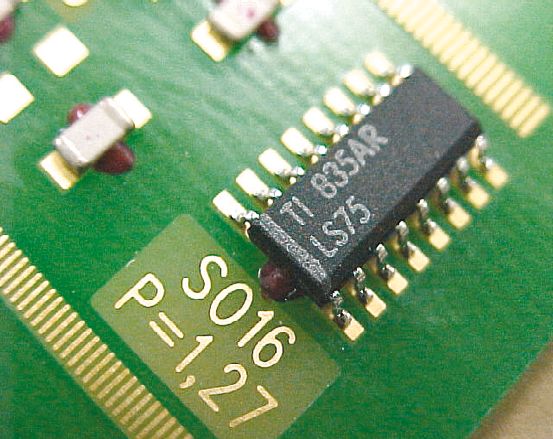
This method can be used providing the solder resist used on the PCB will facilitate the retraction of the paste
deposits during reflow, without leaving isolated satellite solder balls behind.

A simple test utilising either a PCB or portion of salvage can be carried out (see figure 8.17)

                                                                Extent of paste printed off pad

Component hole                                                                                     Isolated solder balls evident after
                                                                                                   reflow (an indication of possible
                                                                                                   solder resist incompatibility)

                                                                                       Solder resist limit

                 Copper pad                                       Figure 8.17 Resist compatibility testing

8.2.1.3 Penetration of paste

This depends largely on the squeegee speed and pressure used. Too quick and the penetration will be restricted,
too high and excessive paste may result. In fact, it isn’t necessary to completely fill the holes with paste, as the
insertion of the component lead will displace a portion of solder paste. Under normal printing conditions with 4-6
kgs pressure and 10-25 mm/second printing speed, a penetration of between 45-85 % can be expected.

Varying these two parameters or overprinting can increase paste penetration. Achieving an average 60% solder
paste penetration will mean a paste depth of nearly 1.0mm on a PCB 1.6mm thick. To achieve this, a reduction
in speed is required from that generally accepted for surface mounting printing where expected paste height is
usually 0.150-0.200 mm.

                                                                                            Figure 8.18 Penetration of paste

8.2.1.4 Component lead length/projection

Lead projection should be kept to between 1.2-
1.5mm when using single thickness stencils with a
maximum of 2.0-2.5mm possible where increased
paste volumes are available using multi-level
stencils.

The component lead will displace a percentage of             > 2.5mm                                                      ≤ 1.25 - 1.5mm
the paste upon insertion with longer pins carrying
paste further away from contributing to the bottom
fillet formation.                                                               ✗                               ✓
                                              Figure 8.19 Lead projection

8    Tecan other stencil applications                                                                                   www.stencils.co.uk
8.2.1.5 Auto insertion / manual insertion

Care should be taken to ensure insertion is carried out as accurately as possible to avoid disturbing or merging
adjacent paste deposits. This is true for both hand and machine insertion. For machine insertion particular
attention should be focused on the ability of the machine to hold or grip the component and on the design or
suitability of the component body itself.

                                                                                        Figure 8.20 Comparison of
                                                                                        bare PCB to printed with
                                                                                        paste for PIHR

There is a noticeable difference between the paste deposits for surface mount devices with the general reduction
in size from the original pad size and the expanded deposits associated with PIHR requirements. With manual
insertion it is necessary for the operator to fully acquaint themselves with the board layout relevant to the
component holes beneath.

Good hand and eye coordination are required to consistently place 96-way connectors, but this can be achieved
with practice.

8.2.2 PIHR component selection

Connectors selected for PIHR should be made of a material capable of surviving reflow without distortion,
melting or cracking. During reflow the connector body will experience temperatures of between 215-230°C
for a period up to one minute. To ensure the connector will survive; it is a good idea to select from a range that
manufacturers qualify to temperatures 20-30°C above peak reflow temperature.

Although it may be possible to adjust the reflow profile to accommodate existing SMT components without
damaging any plastic components, this technique has limited effectiveness.

The solder paste reflows and is attracted towards the hottest points, namely the PCB pads and component leads.
Extended deposits retract to form the required solder fillets.

                                                                Left: Figure 8.21 Paste as printed

                                                                Right: Figure 8.22 Resultant solder fillets post reflow

8.2.2.1 Standoff height/relative position

Suitable components will have built in protrusions on
their underside to maintain a standoff distance.

Printed paste deposits should not be closer than
0.100 mm (0.004”) from the underside of the
component body to avoid possible contamination
of the body with the flux and solder spheres in the
solder paste.
                                                            Figure 8.23 Standoff height

9   Tecan other stencil applications                                                                    www.stencils.co.uk
Select components with standoffs of 0.250-0.325mm (0.010”-0.015”) to avoid contamination and provide
inspection access for the top solder fillets.

Even on simple single row headers, the relative position of the standoff can limit the paste dimensions applied, to
the point where paste volume is not sufficient to form the fillets required. Selection of an alternative component
with in-line standoffs that replaces the crown standoffs (figure 8.25), allows greater flexibility to maximise paste
volume.

Copper pad view from                    Simple expansion of         Consideration of
CAD data.                               paste deposits to achieve   relative standoff        Tailored printing
                                        volumes required.           positions.               solution.

Figure 8.24 Paste deposit expansion

Standoff positions cannot be ignored; they can severely
limit the overall result when their presence impacts on the
stencil design, restricting expansion of the printed paste
deposits and hence paste volume available.

Paste deposits don’t have to be regular shapes to provide              Enlarged paste deposits        Limited paste deposits
the volumes required (See figure 8.26)

Expansion should be limited to no more than 2.5-3.0
times the copper pad diameter in any direction. Ignoring
this can create problems where the solder may not
fully retract on reflow, leaving large solder balls behind
between component terminations.

8.2.3 Pin type

Round, square and oblong pins can all be used, providing a minimum clearance of approximately 0.250mm
(0.010”) exists between the pin and the inside edge of the component holes all around. Too small and insertion
becomes difficult, too large and there may be problems ensuring 100% fill of the holes. When using square or
oblong pins, the hole size should be calculated on the largest dimension plus the required clearance.

                                                                           Figure 8.26 Sufficient clearance surrounding the
                                                                           pin is essential to ensure easy insertion

10   Tecan other stencil applications                                                                            www.stencils.co.uk
8.2.4 Stencil aperture designs
Solder paste, although a complex formulation, follows simple rules upon reflow having similarity to fine pitch
printing where paste deposits should be distinct / isolated to avoid bridging and shorts.
Expanded length and ø deposit
used for single row headers.
Irregular deposit.
Simple expanded deposit used for
test points and widely spaced pins. Figure 8.27 Stencil aperture designs
Teardrop design
Ideal for dual row headers or where restrictions exist
at one end of the pad.
Using PIHR, bridged deposits would leave
the paste confused and unsure where to go
causing fillet variability or large isolated solder
balls.
8.2.4.1 Volume is the result of area and Figure 8.28 Typical elongated Figure 8.29 Resultant paste
thickness PIHR stencil aperture designs deposits
When simply increasing the surface area of a printed deposit does not deliver the volume required, or the gap
between adjacent deposits becomes smaller than 0.250 mm (0.010”), a different approach has to be adopted.
Since PIHR combines existing surface mount technology with leaded components and those leaded components
require more paste, a stencil with thicker areas is required.
Multi-level stencils offer distinct thickness levels on the same stencil, which can be tailored to produce the extra
volumes required for PIHR applications whilst maintaining the appropriate stencil thickness for the surface mount
devices, including fine pitch components.
8.2.4.2 Multi-level stencils / reactivity of squeegee blades
When using multi-level stencils, the squeegee solution must provide the flexibility and small reaction times
required in both the ascent to and descent from the raised areas. Most surface mount assemblies are densely
populated and as such provide only limited clearance between, for example, a large connector and a row
of 0402 components. Recessed or mobile edged squeegee blades are able to offer improved control and
consistency of multi-height printed deposits.
Increased stencil thickness
to provide extra paste volume. Standard stencil thickness Figure 8.30 Recessed edged
for SM devices. squeegee blades and multi-level
stencils
11 Tecan other stencil applications www.stencils.co.uk8.2.5 Reflow reflector shields
Reflow reflector shields (see rework chapter) can be used to maintain
existing reflow profiles whilst using non-reflow capable connectors.
The shield reflects a large proportion of the heat from the sensitive
component body whilst enabling reflow of the soldered terminations.
8.2.6 PIHR results Figure 8.31 Reflow reflector shields
In this section we examine PIHR results with the following components:
• Molex header
• 25-way D-type socket
• 3-pin header
• 6-pin header
• 2-pin header with uncropped legs
• 20-pin DIL socket Figure 8.32 Typical PIHR PCB
assembly
8.2.6.1 Molex header
Body moulding has been removed to examine the resultant solder fillets.
Figure 8.33 Top view Figure 8.34 Bottom view Figure 8.35 Top filets Figure 8.36 Bottom fillets
This component requires a reflow reflector shield to prevent meltdown. As you can see, the solder fillets have a
high wetting angle and the paste has retracted from its printed position without leaving isolated satellite balls.
8.2.6.2 25-way D-type socket
This component also requires a reflow
reflector shield to prevent meltdown. Again,
the solder fillets have a good wetting angle
and there is no evidence of isolated satellite
balls. Figure 8.37 25-way D-type socket
8.2.6.3 3-pin header
Distortion of the plastic body has affected the pin positions.
Figure 8.38 3-pin header
8.2.6.4 6-pin header
This component was reflowed using a reflow reflector
shield. The volume of paste delivered was good, but, this
component is not very well supported and during reflow
it dipped slightly towards the PCB. One answer to this
might be to dispense a glue to maintain its position. Figure 8.39 6-pin header
12 Tecan other stencil applications www.stencils.co.uk8.2.6.5 2-pin inductor with uncropped legs
These were reflowed without the need for shields. Since their lead projection is significant the
solder fillets are depleted by the paste residing on the ends of the component (it is too far away
to retract back to the pads). A possible solution would be to crop before insertion.
8.2.6.6 20-pin DIL socket Figure 8.40 2-pin inductor with uncropped legs
This component was reflowed using a reflow
reflector shield. The volume of paste delivered was good, there are
well-formed solder fillets and no solder ball contamination. As this
component has turned pin legs which are larger on the PCB side
it is not a good idea to force the socket down into the solder paste
as solder bridges may form.
Sockets with turned pins can effectively squash paste into adjacent
deposits. Increased separation between deposits avoids bridging
resulting from insertion.
8.2.7 PIHR summary
PIHR is a technique that utilises existing
production equipment, personnel
and processes and can be employed
successfully provided the basic guidelines
are followed. The calculation and
provision of the appropriate volume of
solder paste to deliver the solder fillets
required, is by far the most important
determining factor to the success of the technique.
Tecan’s CAD engineers calculate the appropriate printed
paste volume to fulfil the solder fillet requirements and will
design the stencil apertures and create any local thickness
increases necessary to ensure your process is successful.
The use of x-ray equipment, although not essential, will
however enable a better understanding of:
• The volume of solder fillet achieved
• Whether the fillet has formed with voids
Figure 8.44 X-ray showing good
hole fill with minimal voids
13 Tecan other stencil applications www.stencils.co.ukYou can also read