Solar Energy Materials and Solar Cells
←
→
Page content transcription
If your browser does not render page correctly, please read the page content below
Solar Energy Materials & Solar Cells 223 (2021) 110945
Contents lists available at ScienceDirect
Solar Energy Materials and Solar Cells
journal homepage: http://www.elsevier.com/locate/solmat
Outdoor performance of a tandem InGaP/Si photovoltaic luminescent
solar concentrator
Megan Phelan a, 1, David R. Needell a, 1, Haley Bauser a, 1, Hanxiao Su b, Michael Deceglie c,
San Theingi c, Brent Koscher d, Zach Nett d, Colton R. Bukowsky a, Ognjen Ilic a, Paul Stradins c,
John Geisz c, Ralph Nuzzo b, A. Paul Alivisatos d, e, Harry A. Atwater a, *
a
California Institute of Technology, Department of Applied Physics and Materials Science, CA, 91125, USA
b
University of Illinois and Urbana-Champaign, Department of Chemistry, IL, 61801, USA
c
National Renewable Energy Laboratory, CO, 80401, USA
d
University of California Berkeley, Department of Chemistry, CA, 94720, USA
e
Lawrence Berkeley National Laboratory, CA, 94720, USA
A R T I C L E I N F O A B S T R A C T
Keywords: We report the design, fabrication and outdoor characterization of a tandem luminescent solar concentrator/Si
Luminescent solar concentrator multi-junction photovoltaic module. Our tandem LSC/Si device consists of an InGaP LSC functioning as a top cell
Tandem photovoltaic and a passivated contact Si bottom cell. The LSC comprises of an InGaP microcell array coupled to a polymer
Quantum dot
waveguide, loaded with CdSe/CdS core-shell quantum dot luminophores. The light trapping efficiency of the LSC
Microcell
Outdoor testing
waveguide is enhanced by encapsulation with photoluminescence trapping mirrors consisting of dielectric
multilayer thin films. We demonstrate the performance of the LSC/Si device through a series of outdoor tests
under various irradiance conditions conducted at the National Renewable Energy Laboratory. We report the first
outdoor testing data of an LSC/Si tandem module, displaying maintained performance across varied diffusivity
conditions for the LSC component. Finally, we model the tandem module performance using a ray optic
simulation-based multiphysics model and forecast a pathway for high efficiency tandem LSC/Si module
performance.
1. Introduction the solar spectrum [6]. Currently, the highest efficiency stabilized
thin-film tandem PV performance has been achieved using III-V com
Traditional flat plate photovoltaic (PV) devices often exhibit incon pound semiconductor tandems, with the highest efficiency devices
stant power conversion under varied illumination conditions. For composed of III-V materials grown on silicon [7]. However, at present,
instance, operation under diffuse lighting conditions can lead to a 20% the costs for III-V materials in thin-film or silicon tandem device con
reduction in power conversion efficiency (PCE) for monocrystalline figurations is too high to be economical for large-scale applications [8].
silicon cells relative to direct solar irradiance [1,2]. Moreover, standard Other pathways for tandem PV devices are being actively explored.
solar radiation data compiled across the United States suggests that Among these, notable high efficiency lead halide perovskite on silicon
diffuse irradiance can compose between 20 and 40% of the global ra tandem prototypes have been reported, although the long-term stability
diation, depending upon geographical region and time of year [3,4]. of these tandem devices is, as of today, unproven [9].
Solar technologies equipped with diffuse-light capture mechanisms An alternative approach to high efficiency tandem modules with
stand to further increase adoption of PV systems. potential to reduce the overall module cost of III-V/Si tandems is to
Considerable research is currently being directed toward developing concentrate incident sunlight onto an array of small III-V micro-cells,
scalable, thin-film tandem or tandem-on-silicon PV cells and modules, thereby minimizing the amount of III-V material required per watt of
which have potential for efficiencies beyond the practical and theoret generated electricity [10,11]. Uniquely among PV concentrators, lumi
ical limits [5] of single-junction devices by utilizing a larger portion of nescent solar concentrators (LSCs) enable concentration of both diffuse
* Corresponding author.
E-mail address: haa@caltech.edu (H.A. Atwater).
1
authors contributed equally to the work.
https://doi.org/10.1016/j.solmat.2020.110945
Received 22 October 2020; Received in revised form 19 December 2020; Accepted 22 December 2020
Available online 10 January 2021
0927-0248/© 2021 Elsevier B.V. All rights reserved.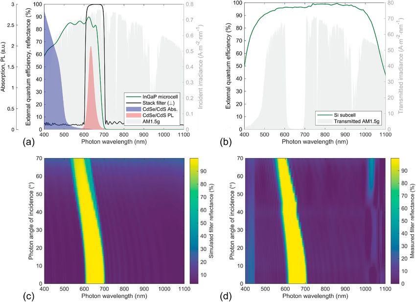
M. Phelan et al. Solar Energy Materials and Solar Cells 223 (2021) 110945
and direct light [10,12]. LSCs can also be developed in flat-plate, fix to increase module efficiencies beyond 30%, well beyond current
ed-axis modules that do not require sun tracking, enabling such tech single-junction performance limits, while dramatically reducing the cost
nology to be particularly suitable to applications of conventional, per watt of the utilized III-V material [11,19].
single-junction PV modules. In an LSC, light is concentrated from a Tandem LSC/Si modules address all critical requirements for tandem
waveguide absorption area, A, to a solar cell collection area, A’; this PV technology implementation: i) functionality in both direct and
ratio of concentration areas is referred to as the geometric gain, where G diffuse lighting conditions, ii) efficient solar spectrum utilization via a
= A/A’ [10]. Functionally, the absorbed incident sunlight is trapped multi-junction module, and iii) reduced materials cost due to integration
within a dielectric waveguide through total internal reflection (TIR). with silicon and the small area fraction for the III-V material (i.e., high
The trapped light is then redirected to small area PV cells for energy GG). In this study, we analyze the first-ever fabricated LSC/Si tandem
conversion. LSCs employ luminophores uniformly dispersed within the module, as shown schematically in Fig. 1. The module consists of (from
waveguide that isotropically absorb high energy photons and re-radiate the top-down): i) a top dielectric aperiodic stack notch filter, ii) a
down-converted photons as photoluminescence (PL) with a high radia polymeric LSC waveguide of poly(lauryl methacrylate) (PLMA) with
tive efficiency, or photoluminescence quantum yield (PLQY). For an uniformly dispersed CdSe/CdS core/shell quantum dots (QDs), iii) an
ideal LSC with a perfect light trapping waveguide, the concentration InGaP III-V micro-cell array, iv) a bottom dielectric aperiodic stack notch
equals the geometric gain (C = G); however, waveguide nonidealities filter, and v) a passivated contact Si subcell. Finally, we supply specular
result in C < G [10]. Initial studies demonstrate the ability of reflective acrylic-Al mirrors along each of the module edges to reduce
stand-alone LSCs to capture both direct and diffuse irradiance, allowing photon losses from edge out-coupling.
sustained performance in varied lighting conditions [13–15]. The con Fig. 1 shows both photographic (Fig. 1a and b) and rendered sche
centration of luminophores dispersed within the waveguide determines matics (Fig. 1c) of the LSC/Si tandem module. Fig. 1d displays a con
the amount of irradiance absorbed, quantified as a spectrally dependent ceptual schematic of the core/shell structure of the CdSe/CdS QDs, as
optical density. Ideal luminophores require a large Stokes shift—the well as a transmission electron microscope (TEM) image of the nano
downshift between absorbed and emitted photon energies—in order to particles. To convert PL (Fig. 1a) into electrical power, we fabricate a
reduce reabsorption losses [16]. PL radiation is trapped within the micro-cell array, composed of embedded III-V InGaP cells with active
waveguide as a result of coupling into guided optical modes, arising areas of 400 μm × 400 μm per cell, shown in the optical microscope
from TIR. Since TIR traps only a portion of the PL, LSCs often employ image in Fig. 1e. We set this array in tandem with a passivated contact
additional external reflectors enclosing the top and bottom surfaces of silicon subcell optimized to harvest long-wavelength photons. Though
the waveguide [17–19]. the embedded InGaP micro-cell planar array occupies a small area
While the performance of single-junction cells has been evaluated fraction, it acts as a PL sink, concentrating QD emitted light to the micro-
under diffuse irradiance conditions using many optical configurations cells. Previous studies have shown the concentration mechanism for
(conventional texture-etched Si cells [20], dielectric nanosphere arrays analogous, single solar cell LSC structures [27–30]. The long wavelength
[21], plasmon nanostructures [22–24], and light trapping wire arrays portion of incident light spectrum not converted into PL is thereby
[25,26]), device performance of tandem LSCs, has not been studied for transmitted to the Si cell. By optically coupling the LSC component to
varied irradiance conditions. Here we investigate designs for III-V/Si the InGaP micro-cell array and matching the PL of the QD luminophores
LSC devices that combine arrays of micro-processed InGaP cells to the InGaP energy bandgap, we concentrate sunlight irradiance in the
embedded within an LSC and optically integrated with a flat plate Si cell ultraviolet/blue part of the spectrum onto high radiative efficiency
for use as a four terminal tandem module. For an optically efficient LSC, InGaP micro-cells to enable higher module efficiency. Our fabricated
the concentration factor can approach the geometrical gain (GG), module is a four terminal structure, reducing the risk of JSC mismatch
defined to be the ratio between the total device illuminated surface area and series resistance between the top LSC and bottom Si. Fig. 1b shows
and the area of the III-V PV material. If high concentration factors the realized LSC-InGaP microcell array that is placed atop the silicon
(>30x) can be achieved, this tandem LSC/Si approach has the potential subcell. The PL of the QD-waveguide under UV-light is shown in Fig. 1a.
Fig. 1. The tandem LSC/Si, four terminal module. (a) The top LSC component consisting of a 4 × 4 InGaP micro-cell array encapsulated within a 30 μm (μm) thick
CdSe/CdS core/shell QD waveguide under UV illumination, visibly displaying PL in the red. (b) The same top LSC component as (a), under ambient light held for
scale. We note that, as viewed in (a) and (b), the right-most column of InGaP micro-cells (4 cells in total) electrically shorted during fabrication process, yielding an
effective 4 × 3 micro-cell array. (c) A 3D rendering of the full tandem LSC/Si module with PL trapping stack filters coupled to the top and bottom surfaces of the LSC
waveguide/InGaP micro-cell array component. (d) The core/shell structure of the CdSe/Cds QDs alongside a transmission electron microscope (TEM) image. (e) A
confocal microscope image of the anchored InGaP micro-cell on the LSC glass substrate, with cell dimensions of approximately 400 μm x 400 μm. (For interpretation
of the references to colour in this figure legend, the reader is referred to the Web version of this article.)
2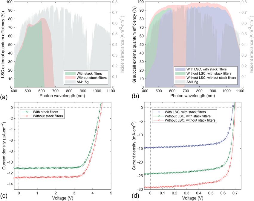
M. Phelan et al. Solar Energy Materials and Solar Cells 223 (2021) 110945
Fig. 2a and b shows the measured, spectral characteristics for the LSC current-voltage (LIV) measurements reveal a JSC = 29.3 mA/cm2 and a
and Si components of the tandem module. The full AM1.5G spectrum VOC = 0.7 V for the bare Si subcell, and a JSC = 12.9 μA/cm2 and a VOC =
impinges upon the top surface of the LSC device. CdSe/CdS QDs absorb 4.5V for the 4 × 3 InGaP micro-cell array under the LSC waveguide.
photons in 400–500 nm wavelength range and photoluminesce at a peak With each layer added to the full device, the total output current from
wavelength of 635 nm, spectrally matching the InGaP electronic the Si is reduced and VOC decreases slightly (Fig. 3c). Additionally, the 4
bandgap (Fig. 2a). This PL is trapped within the waveguide by both TIR × 3 InGaP array experiences a current drop off with the addition of the
and top/bottom notch filters, which reflect photons centered around the top filter (Fig. 3c) as a result of the reduced EQE spectrum of the InGaP
QD PL (Fig. 2a). Incident photons not absorbed by the QDs or reflected micro-cell. However, as discussed later, given proper tuning of the notch
by the notch filters pass through the LSC to the Si subcell. Given the high filter and LSC parameters (e.g., concentrated QD loading, GG), increased
external quantum efficiency (EQE) for the passivated contact Si cell at PL trapping will offset the drop-off in the InGaP micro-cell EQE spectrum
longer wavelengths (Fig. 2b), this design actively splits the incident with the addition of the top filter, thus resulting in an enhanced power
spectrum between high energy photons (LSC) and low energy photons output of the full device.
(passivated contact Si). As shown in Fig. 2b, the transmitted light inci We analyzed the power performance of a fabricated array of 12
dent on the Si subcell is a truncated AM1.5G spectrum due to photons InGaP micro-cells—four cells connected in series across three columns in
that have been either absorbed and trapped by the top LSC component, parallel, spaced 4 mm apart—optically coupled to a QD LSC with an
or reflected by the notch filters. With proper spectral tuning of the notch overall GG of 250. Of note, the 4 × 3 microcell array tested corresponds
filters, increased PL collection by the InGaP micro-cells outweighs filter with a sparser design than is optimal, as shown by the high GG, due to
reflection losses [11]. Fig. 2c and d shows the simulated and measured fabrication challenges of a fully-dense InGaP cell array; for a denser
notch filter reflectance, respectively. In this design we use an aperiodic, array with tighter InGaP cell spacing, we would expect a higher
dielectric layered structure consisting of Ta2O5 (high index) and SiO2 photocurrent density of the LSC top component as discussed in the final
(low index) in order to achieve this notch profile. We observe a close device modeling section. In order to ensure complete optical coupling,
match between simulated and measured transmittance values, with we deposit the LSC QD waveguide directly atop the InGaP micro-cell
slightly lower transmittance in the high photon energy pass band of the array. We show here periodic current-voltage (IV) measurements of
fabricated mirror owing to absorption from the thick, 2 mm glass sub the LSC/Si tandem module throughout an outdoor field test performed
strate of the dielectric stack. in the week of November 12th, 2018 at the National Renewable Energy
We conducted indoor laboratory measurements, taken under one- Laboratory (NREL) in Golden, CO. In addition, we simulated loss
sun solar simulation, to reveal the optical properties of each compo mechanisms intrinsic to this design via a Monte Carlo ray-tracing algo
nent in the module. Fig. 3a and b illustrate the effects of individual LSC rithm. We spatially mapped the PL collection of a single InGaP micro-
components on the EQE performance in an analogous layer-by-layer cell within the QD waveguide to determine photon travel distances
fashion. As the LSC components shape the incident light spectrum, within the LSC to further analyze efficiency loss mechanisms. Finally, we
fewer photons are collected by the Si subcell, as seen in Fig. 3b. Light designed and optimized the tandem LSC/Si module addressing each
Fig. 2. The spectral characteristics of the tandem LSC/Si module. (a) The top LSC PV component, comparing the spectra of the absorption/PL of the CdSe/CdS QDs
(far left y-axis), the external quantum efficiency (EQE) of the anchored InGaP micro-cell (left y-axis), the stack filter reflectance spectrum at normal incidence (left y-
axis), and the incident AM1.5G spectrum (right y-axis). (b) The bottom Si component of the tandem LSC/Si module, comparing the spectra of the passivated contact
Si cell EQE (left y-axis) against the transmitted irradiance through the LSC component (right y-axis). (c), (d) The simulated and measured dielectric, aperiodic stack
filter with alternating layers of Ta2O5 and SiO2, respectively. The realized stack filter (d) is deposited atop an approximately 2 mm thick glass substrate.
3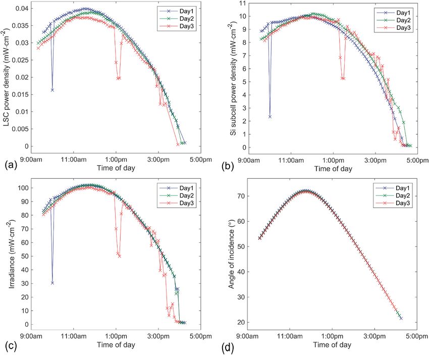
M. Phelan et al. Solar Energy Materials and Solar Cells 223 (2021) 110945
Fig. 3. The measured electrical performance of the tandem LSC/Si device under artificial, AM1.5G light via a solar simulator. (a) The EQE analysis for the top LSC
component for the cases with and without PL-trapping stack filters. (b) The EQE analysis for the bottom, passivated contact Si component for the cases with the LSC
and PL-trapping stack filters, with only the stack filters, and finally without the LSC or the filters. (c) Light IV measurements of a sparse InGaP micro-cell array top
LSC component for the cases with and without PL-trapping stack filters, under AM1.5G illumination. (d) Light IV measurements of the Si passivated contact bottom
cell for the same cases as in (b), under AM1.5G illumination.
identified loss mechanism and sources of inefficiency to forecast the deposited on top of a soda-lime glass substrate of 2.5 cm × 2.5 cm. A
performance limits for such tandem module designs. polydimethylsiloxane (PDMS) stamp was then used to transfer the
micro-cells, isolated by the RIE etching process, to the glass substrate
2. Methods and module fabrication deterministically to form an array of cells [34,35]. The SOG-E layer was
cured by sequential heating and UV exposure. The edges of the cells
Upright n-on-p InGaP solar cells were grown on GaAs substrates by were insulated with SU-8 2025 to avoid shorting. A Cr/Cu/Al/Au
atmospheric-pressure metal-organic vapor phase epitaxy (MOVPE) [31, interconnect was then sputtered to complete the array.
32]. The Zn-doped absorber layer was approximately 900 nm thick with To obtain high luminophore spectral performance, we fabricated
a 2 μm Al.5Ga.5As lateral conduction layer (LCL) for transparency, which CdSe/CdS core/shell QDs closely following literature procedures [19].
allowed bifacial operation of the device. An AlInP layer was used Absorption spectra were measured using a Shimadzu UV-3600 double
beneath the LCL as a sacrificial layer for lifting off micro-cells during beam spectrometer. Measurements were conducted at dilute concen
transfer printing. For the fabrication of micro-cells, the geometry of the trations to minimize the influence of scattering. PL spectra were
n-contact was first defined via photolithography. A contact layer with measured using a Horiba Jobin-Yvon FluoroLog steady-state spectro
10 nm of Ni and 1 μm of Au was then electrodeposited. The cell mesa was fluorometer, exciting above the bandgap at 430 nm. The detection PMT
defined with a two-step wet etch, the first being a 1:100 of the spectrofluorometer was calibrated for spectral sensitivity. For
bromine-hydrobromic (48% HBr, Sigma-Aldrich) acid etch, to TEM analysis, dilute solutions of the nanocrystal stock solution were
non-selectively complete the main part of the etch; the second being a drop cast onto TEM grids (Electron Microscopy Sciences CF400–Cu).
saturated HCl etch, to selectively remove the remaining InGaP and Multiple TEM images with thousands of quantum dots were sized using
expose a smooth, undamaged LCL. The p-contact was deposited simi an automated analysis script to ensure consistency from the nanoparticle
larly, and the devices were isolated by another HCl etch, exposing the synthesis.
GaAs substrate. Silicon nitride was deposited over the device via We dispersed core/shell QD particles within the monomers lauryl
plasma-enhanced chemical vapor deposition (PECVD) to reduce Fresnel methacrylate (LMA, Sigma-Aldrich) and ethylene glycol dimethacrylate
losses and non-radiative recombination. Contact windows and lift-off (EGDMA, Sigma-Aldrich) at a 10:1 ratio. Darocur 1173 (Sigma-Aldrich)
edges were opened via CF4 reactive ion etch (RIE). A secondary photoinitiator was added at 0.05% volume. We placed 30 μm, soda-lime
on-cell Au contact was deposited by sputtering. Photoresist was used to glass spacers atop the 2.5 cm × 2.5 cm glass substrate (hosting the InGaP
anchor the cells for lift off. A 1:4 HCl–H2O etchant was used to remove micro-cell array) and mounted a capping, quartz glass superstrate atop
the sacrificial layer. the spacers, treated with repel-silane (GE Healthcare). To obtain a 30 μm
A 150 nm layer of spin-on-glass/epoxy (SOG-E) adhesive [33] was waveguide thickness, we applied a capillary force method, injecting the
4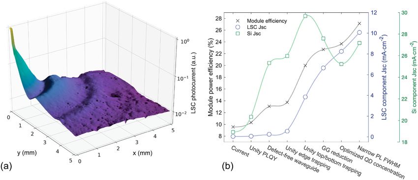
M. Phelan et al. Solar Energy Materials and Solar Cells 223 (2021) 110945
QD/monomer solution between the glass substrate/InGaP array and the reflectance and internal quantum efficiency of both the silicon subcell
glass superstrate. We cured the QD/monomer solution under 365 nm UV and InGaP micro-cell to determine the amount of generated photocur
exposure, afterwards the quartz glass superstrate can be removed after rent within each cell type. All photons simulated terminate in either
curing, as the repel-silane surface treatment prevents strong bonding to collection by one of the two cell types or termination by one of the loss
the polymer waveguide. mechanisms, as discussed in Fig. 6. All details regarding the algorithm,
We designed and optimized the dielectric, aperiodic notch filter stack implementation, and model validation to experimental studies can be
following a previously used optimization procedure [11]. We fabricated found in previous studies by Needell et al. [38] and Bronstein et al. [27].
the stack filter onto a 2.5 cm × 2.5 cm x 2 mm glass substrate with an
anti-reflective coating opposite the dielectric stack (Evaporated Coat 3. Outdoor testing results
ings Inc., Willow Grove, PA USA). We mechanically stacked the InGaP
array/LSC component directly on the bottom dielectric stack filter and We determined the effects of irradiance and diffuse light illumination
glass substrate. We similarly placed the top dielectric filter atop the on tandem LSC/Si performance through outdoor field testing, with
PLMA-QD waveguide to complete our device design. Finally, we placed modules tilted at a fixed 40◦ relative to horizontal with continuous on-
this bottom filter/InGaP micro-cell array/PLMA-QD waveguide/top site irradiance measurements [39]. We found that power output as a
filter structure atop a passivated contact Si cell with a window area of function of the time-of-day (Fig. 4a and b) achieves its maximum per
1.6 cm × 2.5 cm. formance near 12:00 p.m. As seen in Fig. 4a and b, this maximum power
Our bottom Si subcell is a single side textured, rear junction cell with for both components coincides with maximum solar irradiance (Fig. 4c)
heavily doped n-type and p-type poly-Si/SiOx passivation layers as well as an angle of incidence nearest to normal incidence of the
deposited at the front and the back of an n-type Cz wafer respectively. module (Fig. 4d) given the tilted axis of the field-test. The supporting
First, 170 μm thick, single side textured, 2.5–3 Ohm cm n-Cz wafers were information details the direct affect of angle of incidence on both LSC
cleaned using piranha, standard RCA 1 and RCA 2 process. Then, and Si subcell device power output. By 4:00 p.m. and onwards, limited
approximately 1.5 nm thick low temperature thermal tunneling SiOx incident irradiance and large off-normal angle of incidence results in
was grown on an RCA cleaned single side textured n-Cz wafer. A 50 nm negligible output power of the module. We observe similar temporal
thick PECVD grown n-type and p-type doped hydrogenated amorphous trends for both the Si subcell and the LSC top cell. Shown in Fig. 4a, the
silicon (a-Si:H) was then deposited on top of this tunneling oxide. The maximum power output decreases across the LSC over the course of the
sample was placed inside a diffusion furnace in an N2 environment at three testing days, a trend not seen in the Si subcell power output vs.
850C for 30 min to simultaneously diffuse the dopants and crystallize time-of-day (Fig. 4b). Such a power decrease implies a degradation
amorphous Si to polycrystalline Si. 15 nm of alumina oxide is then added mechanism of the LSC component itself, most likely attributed to pho
using atomic layer deposition and is activated at 400C in a forming gas todegradation of the PLQY of the luminophores [40,41].
environment to enhance the passivation. The resulting cell has a One of the most promising features of such an active concentrator
passivation that can reach above 730 mV in iVoc and ~10 fA/cm2 J0 LSC design results from the sustained functionality in both direct and
values. The metal contacts were formed by thermally evaporating tita diffuse illumination conditions. Shown in Fig. 5a, we demonstrated
nium and silver through the openings of a shadow mask. We soldered outdoor field testing data that is consistent with the PCE trends found in
metal ribbons to the pads at the end of the busbar and the back contact to previous work for LSCs [13] as well as for simulated tandem LSC/Si
provide electrical leads for the tandem configuration [36]. devices operating under varied diffuse and direct irradiance conditions
The passivated contact Si cell was measured using a solar simulator [11]. Seen in Fig. 5b, the Si subcell power conversion efficiency begins to
under 1 sun condition and then measured again under the CdSe/CdS monotonically decrease once the amount of DNI light drops below 50
waveguide and bottom filter stack to estimate the performance of the mW/cm2. In contrast, the top LSC component does not demonstrate a
cell in the LSC/Si configuration. Under 1 sun, the cell achieves Voc of steady decreasing trend in PCE as a function of DNI. Of note, the slight
703.2 mV, Jsc 38.9 mA/cm2, and an efficiency of 20.6%. When this cell is spread in normalized efficiency for both the LSC and Si components in
measured under the waveguide and the filter stack, the Voc of the cell Fig. 5b is due to discrete trends associated with each day’s data collec
decreases to 694 mV, and Jsc to 27.3 mA/cm2 due to the reduced inci tion. These spreads may be a result of the day-to-day variations in testing
dent illumination on the cell, resulting in an efficiency of 14.4% for Si conditions. Moreover, we hypothesize that the slight drop in normalized
subcell. We encapsulate this Si subcell with a mm-thick layer of Poly efficiency for the Si subcell towards maximum DNI * Irradiance of 100,
dimethylsiloxane (PDMS). In order to approximate a large-area III-V which typically occurs near noon, may result from the change of the
micro-cell array via side loss reduction, we place this tandem LSC/Si solar spectrum after noon. Fernandez et al. have shown that higher
device within a mirrored acrylic test bed [37]. We measure the reflec angles of incidence, as occur in the afternoon, produce a larger attenu
tance of this rectangular trench with a Varian Cary 5G UV–Vis ation of the UV–visible region of the spectrum, resulting in a red-shifted
spectrophotometer. spectrum [42]. A red-shifted solar spectrum is better matched to the
We apply a Monte Carlo, ray-tracing model to stochastically simulate silicon band edge, potentially leading to a slight increase in perfor
the performance (photocurrent, Jsc) of this four terminal, tandem LSC/Si mance, as seen in Fig. 5b.
device. We initialize greater than 2 × 10⁶ individual photons to strike
the top surface of the tandem module, spectrally distributed between the 4. Device performance analysis
wavelengths of 300–1500 nm, and spatially segmented given a mesh
grid of 25 μm over the top surface area. We trace each photon Our device underperforms previous simulated work of an LSC/Si
throughout the device, keeping track of the current and previous posi tandem design, which suggests an optimized LSC/Si tandem module can
tions, current and past wavelengths, current and past photon velocity reach power conversion efficiencies near 29% [11]. In this study, the Si
vectors, and photon polarization. We apply the Beer-Lambert law given subcell—when integrated in the LSC/Si tandem module—performed at a
the QD concentration within the PLMA waveguide (via the measured 10% PCE, and the LSC component contributed 0.04% PCE. To identify
optical density) to determine the probability of photon absorption via loss mechanisms and optimize our design performance, we simulated
dispersed luminophores for a given photon step. We apply Snell and the LSC/Si tandem module design with a Monte Carlo ray-tracing al
Fresnel laws to determine the trajectory of each photon upon change of gorithm and detailed balance model in order to observe how experi
refractive index and material interaction. We apply the measured mental data match with model predictions. Previous work shows this
transmittance and reflectance of the top/bottom PL filters with respect model to be in strong agreement with experimental observation [38].
to wavelength and angle of incidence within the model to determine the We applied this computational tool to understand the causes of lowered
interaction of photons with these layers. Finally, we implement the output current by the top LSC component. Fig. 6 illustrates the primary
5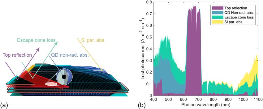
M. Phelan et al. Solar Energy Materials and Solar Cells 223 (2021) 110945
Fig. 4. Outdoor testing results with respect to time of day at the National Renewable Energy laboratory in Colorado, USA for November 13th, 14th, and 15th 2019.
(a) The top LSC component and (b) the bottom Si cell component power output in mW per cm2 over the course of three full days of testing. (c) The solar irradiance
(mW per cm2) and (d) angle of incidence (AoI) (degrees) relative to the modules’ top surface for each day of testing, where 90 degrees signifies normal incidence.
Dips in the data correspond to brief periods of cloud and/or snow coverage at the testing facility.
Fig. 5. Outdoor testing results with respect
to direct normal irradiance (DNI) at the
National Renewable Energy laboratory in
Colorado, USA for November 12th (partial
day), 13th, 14th, 15th, and 16th 2019. Here
we show the normalized efficiency for the
(a) top LSC component and (b) bottom Si
component. We normalize each individual
day’s power conversion efficiency to the
highest efficiency for that given day. Days 3
and 4 of (a) correspond to the case with no
top PL-trapping stack filter.
loss mechanisms that limit the performance of such a tandem structure. schematically and spectrally in Fig. 6a and b, respectively.
We found the most significant areas of photon loss stem directly from: i) In the short wavelength regime (wavelengths below the notch filter
top filter reflection of incident irradiance, ii) non-radiative recombina stop-band), the primary loss mechanism results from non-radiative QD
tion of absorbed photons by the QD luminophores (i.e., non-unity absorption due to non-unity PLQY. From ray-tracing simulations and
PLQY), iii) scattered photons lost through the escape cone of the performance matching to outdoor data, we found QD PLQYs to decrease
waveguide/filter component, and iv) parasitic Si subcell absorption (e. down to approximately 60% over the course of the testing period. As
g., incomplete light coupling into the wafer by the front texture and shown in Fig. 4a, we found that the power output of the LSC degraded
antireflective coating (ARC), absorption of the trapped near infrared steadily over each day, implying potential generation of defects in QDs
(NIR) light by the back reflector). We illustrate such loss mechanisms within the waveguide performance, which we attribute to decreasing
6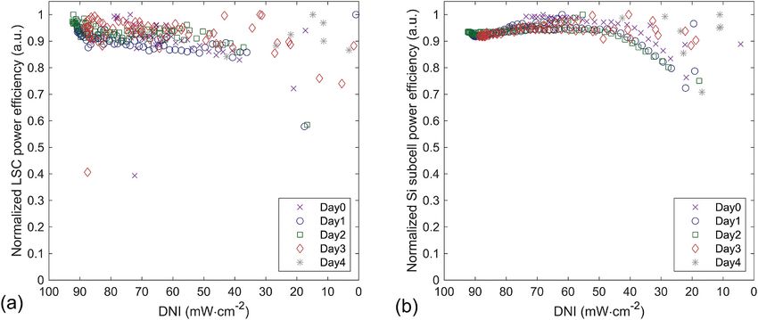
M. Phelan et al. Solar Energy Materials and Solar Cells 223 (2021) 110945
Fig. 6. Computational results showing the
primary loss mechanisms responsible for
underperformance in the tandem LSC/Si
system. (a) A rendered schematic depicting
the various loss mechanisms, including: top
surface reflection of incident sunlight due,
primarily, to the top notch filter (purple),
escape cone loss from the LSC waveguide
(green), QD non-radiative recombination
absorption (blue), and Si parasitic absorp
tion (yellow). (b) The spectral account for
the full tandem LSC/Si loss mechanisms,
given as the total lost photocurrent (amps
per m2 per nm). (For interpretation of the
references to colour in this figure legend, the
reader is referred to the Web version of this
article.)
QD PLQY. As the LSC PLQY degrades, the probability of photon loss due into a spatial quadrant analyzing a 2.5 cm × 2.5 cm waveguide area
to QD absorption increases, thereby causing decreased power output. —equivalent to a GG of 625—shown in Fig. 7a. As seen, the measured
For wavelengths within the stop-band of the filters, reflection due to photocurrent drops with the spatial separation between the illumination
this spectral feature is the main cause of photon loss. While the near- point and the micro-cell corner. An inflection point in the steep drop off
perfect reflectance from the notch filter around the 600–700 nm spec located less than 0.2 mm from the quadrant origin indicates a combi
tral range increases PL trapping and photocurrent delivery to the InGaP nation of PL and nearby scattered, short wavelength light collected in
micro-cells within the LSC waveguide, it also prevents photons within this small radius. Such an inflection reveals that the mean photon travel
this frequency range to be transmitted through the top surface to reach distances within the LSC waveguide are significantly limited by a
either the InGaP array or Si subcell. With near-unity PLQY QDs, PL convolution of escape-cone and non-radiative QD losses.
trapping within the LSC outweighs the reflected incident photon loss Via an understanding of the loss mechanisms in the LSC, we can
within this wavelength range. The finite top-filter reflectance below 500 design an improved tandem device. Fig. 7b projects the modeled power
nm light correspondingly reduces the produced PL. Improved filters conversion efficiency, as well as the associated photocurrents for each
could increase spectral transmission down to at least 400 nm and the LSC top component and Si subcell, possible for various approaches to
enhance QD photon absorption. Another cause of decreased LSC component optimization for the tandem LSC device under ideal condi
photocurrent results from PL photon loss through the escape cone of the tions (e.g., normal incidence sunlight). One promising method for
PLMA waveguide due to top filter transmission. Peak filter reflectivity maintaining QD stability and enhancing PLQY performance involves the
blue-shifts with angles of incidence as illustrated in Fig. 2c and d. PL that use of siloxane as a part of the waveguide matrix, which has shown to
scatters or emits into larger angles of the waveguide escape cone help QDs maintain PLQY across high temperature and various moistures
decreasingly reflects back into trapped modes. Finally, a fraction of the due to the strong thermal stability of the bonds in the siloxane [45]. In
low energy photons (λ > 900 nm) collected by the Si subcell is lost due to Fig. 7b, we model the following optimizations: i) unity PLQY, improved
parasitic absorption. from the current modeled conditions of 60%, ii) a defect free waveguide,
As shown in the photocurrent loss mechanisms in Fig. 6b, QD non- consisting of an increased quality factor of the QDs, defined as the ratio
radiative absorption and waveguide escape cone re-emission account of absorption at the band edges of CdSe to CdS [46], and non-aggregated
for a vast portion of loss mechanisms for the LSC component. Improved dispersion of luminophores within the polymer [47]; iii) minimized PL
PL collection requires increased optical efficiency of the waveguide leakage from the device edges; iv) optimized top/bottom filters to
[43]. We spatially mapped the photoluminescence emission within the reduce loss from low-wavelength incident photon reflection and scat
waveguide by scanning a 490 nm wavelength, 10 μm spot-size beam tered photon transmission through the waveguide escape cone; v) a
[44] across an analogous single InGaP micro-cell LSC. We illuminated decreased geometric gain (from 250 to 10) of the LSC for higher PL
the waveguide from the corner of the 0.16 mm2 micro-cell and extend micro-cell collection yields, without obscuring long-wavelength photons
Fig. 7. (a) The photocurrent mapping of a
single InGaP micro-cell embedded within a
30 μm waveguide doped with CdSe/CdS QDs
plotted on a log scale. A 490 nm laser source
scans x- and y-distances up to 5 mm from the
outside corner of the device active area (the
origin corresponding to the cell center). (b)
A performance forecast for the tandem LSC/
Si module, illustrating approaches for
increased module power efficiency (left y-
axis, black x-markers) through optimization
of the LSC component, alongside the pre
dicted LSC photocurrent (right y-axis, blue
circle-markers) and predicted Si subcell
photocurrent (far right y-axis, green square-
markers). Efficiencies are modeled for 100%
DNI under standard AM1.5G conditions.
(For interpretation of the references to
colour in this figure legend, the reader is
referred to the Web version of this article.)
7
M. Phelan et al. Solar Energy Materials and Solar Cells 223 (2021) 110945
from reaching the Si component; vi) a re-optimized concentration (i.e., No. DE-AC36-08GO28308. Funding was provided by ARPA-E. The views
optical density) of the QDs within the waveguide (from 0.33 to 2.4 at expressed in the article do not necessarily represent the views of the DOE
450 nm); and vii) a decreased QD PL full-width at half-maximum or the U.S. Government. The U.S. Government retains and the publisher,
emission profile [48]. As shown, waveguide defects (e.g., PL scat by accepting the article for publication, acknowledges that the U.S.
tering) marginally affect the LSC performance as a detriment, which is Government retains a nonexclusive, paid-up, irrevocable, worldwide
consistent with previous literature on scattering within CdSe/CdS license to publish or reproduce the published form of this work, or allow
luminophore matrices [27]. By optimizing for each of these components, others to do so, for U.S. Government purposes.
the tandem device is expected to achieve an ultimate output photocur
rent of 10.1 mA/cm2 and VOC = 1.48V for the LSC component with 27.2 Appendix A. Supplementary data
mA/cm2 and VOC = 0.65V for the Si subcell. These optimizations are
predicted to enable a total module power efficiency of 27.2% under Supplementary data related to this article can be found at https
1-sun illumination, matching previous simulated work given the device ://doi.org/10.1016/j.solmat.2020.110945.
spectral characteristics [11,38]. Given this design, tandem LSC/Si de
vices show promise as a high PCE tandem device with sustained per References
formance in highly diffuse settings.
[1] B. Herteleer, J. Cappelle, J. Driesen, Quantifying low-light behaviour of
photovoltaic modules by identifying their irradiance- dependent efficiency from
5. Summary and conclusion data sheets, in: 27th European Photovoltaic Solar Energy Conference, 2012,
pp. 3714–3719.
We report an LSC/Si tandem module that demonstrates maintained [2] M. Donovan, B. Bourne, J. Roche, Efficiency vs. irradiance characterization of PV
modules requires angle-of-incidence and spectral corrections, Conf. Rec. IEEE
performance under variable diffusivity conditions. Through outdoor Photovolt. Spec. Conf. (2010) 2301–2305, https://doi.org/10.1109/
testing at NREL (Golden, CO), we measure the effects of diffuse irradi PVSC.2010.5615838.
ance on performance of each the LSC top-component and Si subcell. In [3] J.L. Kafka, M.A. Miller, A climatology of solar irradiance and its controls across the
United States: implications for solar panel orientation, Renew. Energy 135 (2019)
addition, we simulate a tandem LSC using a Monte Carlo ray-tracing
897–907, https://doi.org/10.1016/j.renene.2018.12.057.
model to quantify the various loss mechanisms present in the module [4] C.A. Gueymard, Fixed or tracking solar collectors? Helping the decision process
design. We finally forecast that a tandem LSC has the potential to ach with the solar resource enhancement factor, Opt. Model. Meas. Sol. Energy Syst. II
7046 (2008) 70460D, https://doi.org/10.1117/12.795506. September 2008.
ieve up to 27.2% power conversion efficiency— a significant efficiency
[5] W. Shockley, H.J. Queisser, Detailed balance limit of efficiency of p-n junction
increase with respect to the baseline 20.6% efficient Si-only cell under solar cells, J. Appl. Phys. 32 (3) (1961) 510–519, https://doi.org/10.1063/
100% direct normal irradiance—while further maintaining performance 1.1736034.
across varied DNI conditions. [6] M.A. Green, et al., Solar cell efficiency tables (version 50), Prog. Photovoltaics Res.
Appl. 25 (7) (2017) 668–676, https://doi.org/10.1002/pip.2909.
[7] M.A. Green, et al., Solar cell efficiency tables (Version 53), Prog. Photovoltaics Res.
CRediT authorship contribution statement Appl. 27 (1) (2019) 3–12, https://doi.org/10.1002/pip.3102.
[8] J.S. Ward, et al., Techno-economic analysis of three different substrate removal and
reuse strategies for III-V solar cells, Prog. Photovoltaics Res. Appl. 24 (2016)
Megan Phelan: Conceptualization, Methodology, Data collection, 1284–1292, https://doi.org/10.1002/pip.
Writing - original draft. David R. Needell: Conceptualization, Meth [9] P.S.C. Schulze, et al., 25.1% high-efficiency monolithic perovskite silicon tandem
odology, Data collection, Writing - original draft. Haley Bauser: solar cell with a high bandgap perovskite absorber, Sol. RRL 4 (7) (2020) 1–10,
https://doi.org/10.1002/solr.202000152.
Conceptualization, Methodology, Data collection, Writing - review & [10] M.G. Debije, P.P.C. Verbunt, Thirty years of luminescent solar concentrator
editing. Hanxiao Su: Methodology, Data collection. Michael Deceglie: research: solar energy for the built environment, Adv. Energy Mater. 2 (1) (2012)
Data collection. San Theingi: Methodology, Data collection. Brent 12–35, https://doi.org/10.1002/aenm.201100554.
[11] D. R. Needell et al., “Design criteria for micro-optical tandem luminescent solar
Koscher: Methodology, Data collection. Zach Nett: Methodology, Data concentrators,” IEEE J. Photovoltaics, vol. 8, no. 6, pp. 1560–1567, Nov. 2018, doi:
collection. Colton R. Bukowsky: Data collection. Ognjen Ilic: Meth 10.1109/JPHOTOV.2018.2861751.
odology, Data collection. Paul Stradins: Conceptualization, Methodol [12] M. Carrascosa, S. Unamuno, Monte Carlo simulation of the performance of PMMA
luminescent solar collectors, Appl. Optic. 22 (20) (1983) 3236–3241.
ogy. John Geisz: Conceptualization, Methodology, Data collection.
[13] M.G. Debije, V.A. Rajkumar, Direct versus indirect illumination of a prototype
Ralph Nuzzo: Conceptualization, Methodology. A. Paul Alivisatos: luminescent solar concentrator, Sol. Energy 122 (2015) 334–340, https://doi.org/
Conceptualization, Methodology. Harry A. Atwater: Conceptualiza 10.1016/j.solener.2015.08.036.
tion, Methodology, Writing - review & editing. [14] A.J. Chatten, K.W.J. Barnham, B.F. Buxton, N.J. Ekins-Daukes, M.A. Malik, A new
approach to modelling quantum dot concentrators, Sol. Energy Mater. Sol. Cells 75
(3–4) (2003) 363–371, https://doi.org/10.1016/S0927-0248(02)00182-4.
Declaration of competing interest [15] V. Wittwer, W. Stahl, A. Goetzberger, Fluorescent planar concentrators, Sol. Energy
Mater. 11 (3) (1984) 187–197, https://doi.org/10.1016/0165-1633(84)90070-4.
[16] E. Yablonovitch, Thermodynamics of the fluorescent planar concentrator, J. Opt.
The authors declare that they have no competing interests with Soc. Am. 70 (11) (1980) 1362–1363, https://doi.org/10.1364/josa.70.001362.
respect to this manuscript. [17] D.K.G. de Boer, Optimizing wavelength-selective filters for luminescent solar
concentrators, Sol. Energy 7725 (2010), https://doi.org/10.1117/12.853846,
77250Q-77250Q–9.
Acknowledgments [18] R. Connell, C. Pinnell, V.E. Ferry, Designing spectrally-selective mirrors for use in
luminescent solar concentrators, J. Optic. 20 (2) (2018), https://doi.org/10.1088/
This work was supported in part by the Advanced Research Projects 2040-8986/aaa074.
[19] N.D. Bronstein, et al., Quantum Dot Luminescent Concentrator Cavity Exhibiting
Agency for Energy (ARPA-E, U.S. Department of Energy Micro-scale 30-fold Concentration, ” ACS Photonics, 2015, https://doi.org/10.1021/
Optimized Solar-cell Arrays with Integrated Circuits (MOSAIC) Award acsphotonics.5b00334, 150821134054007.
DE-AR0000627, and in part by the Engineering Research Center Pro [20] J. Kim, D. Inns, K. Fogel, D.K. Sadana, Surface texturing of single-crystalline silicon
solar cells using low density SiO 2 films as an anisotropic etch mask, Sol. Energy
gram of the National Science Foundation and the Office of Energy Effi Mater. Sol. Cells 94 (2010) 2091–2093, https://doi.org/10.1016/j.
ciency and Renewable Energy of the Department of Energy under NSF solmat.2010.06.026.
Cooperative Agreement No. EEC-1041895. The authors thank Joshua [21] J. Grandidier, et al., Solar cell efficiency enhancement via light trapping in
printable resonant dielectric nanosphere arrays, Phys. Status Solidi Appl. Mater.
Morse for his expertise in the outdoor testing facility setup, Waldo
Sci. 210 (2) (2013) 255–260, https://doi.org/10.1002/pssa.201228690.
Olavarria for OMVPE growth of GaInP cells, and the Resnick Institute for [22] R.H. Fan, et al., Broadband antireflection and light-trapping enhancement of
Sustainability at the California Institute of Technology for their plasmonic solar cells, Phys. Rev. B Condens. Matter 87 (19) (2013) 1–7, https://
continued support. This work was authored in part by the National doi.org/10.1103/PhysRevB.87.195444.
[23] J.N. Munday, H.A. Atwater, Large integrated absorption enhancement in
Renewable Energy Laboratory, operated by Alliance for Sustainable plasmonic solar cells by combining metallic gratings and antireflection coatings,
Energy, LLC, for the U.S. Department of Energy (DOE) under Contract Nano Lett. 11 (6) (2011) 2195–2201, https://doi.org/10.1021/nl101875t.
8
M. Phelan et al.                                                                                                                    Solar Energy Materials and Solar Cells 223 (2021) 110945

[24] V.E. Ferry, L.A. Sweatlock, D. Pacifici, H.A. Atwater, Plasmonic nanostructure                      concentrators, Opt. Mater. 42 (2015), https://doi.org/10.1016/j.
     design for efficient light coupling into solar cells vivian, Nano Lett. 8 (12) (2008)               optmat.2015.02.011.
     4391–4397.                                                                                   [38]   D. R. Needell, C. R. Bukowsky, S. Darbe, H. Bauser, O. Ilic, and H. A. Atwater,
[25] S.W. Boettcher, et al., Energy-conversion properties of vapor-liquid-solid-grown                    “Spectrally matched quantum dot photoluminescence in GaAs-Si tandem
     silicon wire-array photocathodes, Science 84 327 (5962) (2010), https://doi.org/                    luminescent solar concentrators,” IEEE J. Photovoltaics, vol. 9, no. 2, pp. 397–401,
     10.1126/science.1180783, 185–7.                                                                     Mar. 2019, doi: 10.1109/JPHOTOV.2019.2892075.
[26] M.D. Kelzenberg, et al., Enhanced absorption and carrier collection in Si wire               [39]   I.M. Slauch, M.G. Deceglie, T.J. Silverman, V.E. Ferry, et al., Outdoor Testing of c-
     arrays for photovoltaic applications, Nat. Mater. 9 (3) (2010) 239–244, https://doi.                Si Photovoltaic Modules with Spectrally-Selective Mirrors for Operating
     org/10.1038/nmat2635.                                                                               Temperature Reduction, 46th IEEE Photovolt. Spec. Conf. (2019) 112–117,
[27] N.D. Bronstein, et al., Quantum dot luminescent concentrator cavity exhibiting 30-                  https://doi.org/10.1109/PVSC40753.2019.8981160.
     fold concentration, ACS Photonics 2 (11) (2015) 1576–1583, https://doi.org/                  [40]   R. An, et al., Photostability and photodegradation processes in colloidal CsPbI3
     10.1021/acsphotonics.5b00334.                                                                       perovskite quantum dots, ACS Appl. Mater. Interfaces 10 (45) (2018)
[28] H.-J. Song, B.G. Jeong, J. Lim, D.C. Lee, W.K. Bae, V.I. Klimov, Performance limits                 39222–39227, https://doi.org/10.1021/acsami.8b14480.
     of luminescent solar concentrators tested with seed/quantum-well quantum dots in             [41]   T. Aubert, et al., Bright and stable CdSe/CdS@SiO2nanoparticles suitable for long-
     a selective-reflector-based optical cavity, Nano Lett. 18 (1) (Jan. 2018) 395–404,                  term cell labeling, ACS Appl. Mater. Interfaces 6 (14) (2014) 11714–11723,
     https://doi.org/10.1021/acs.nanolett.7b04263.                                                       https://doi.org/10.1021/am502367b.
[29] N.D. Bronstein, et al., Luminescent solar concentration with semiconductor                   [42]   E.F. Fernández, F. Almonacid, P.M. Rodrigo, P.J. Pérez-Higueras, CPV systems, in:
     nanorods and transfer-printed micro-silicon solar cells, ACS Nano 8 (1) (Jan. 2014)                 McEvoy’s Handbook Of Photovoltaics: Fundamentals and Applications, Elsevier
     44–53, https://doi.org/10.1021/nn404418h.                                                           Inc., 2018, pp. 931–985.
[30] X. Sheng, et al., Doubling the power output of bifacial thin-film GaAs solar cells by        [43]   W.G.J.H.M. Van Sark, Z. Krumer, C.D.M. Donegá, R.E.I. Schropp, “Luminescent
     embedding them in luminescent waveguides, Adv. Energy Mater. 3 (8) (Aug. 2013)                      solar Concentrators : the route to 10 % efficiency, IEEE J. Photovoltaics, 2014,
     991–996, https://doi.org/10.1002/aenm.201201064.                                                    pp. 2276–2279.
[31] S. Essig, et al., Raising the one-sun conversion efficiency of III-V/Si solar cells to       [44]   D. Fleischman, K.T. Fountaine, C.R. Bukowsky, G. Tagliabue, L.A. Sweatlock, H.
     32.8% for two junctions and 35.9% for three junctions, Nat. Energy 2 (9) (2017),                    A. Atwater, High spectral resolution plasmonic color filters with subwavelength
     https://doi.org/10.1038/nenergy.2017.144.                                                           dimensions, ACS Photonics 6 (2019) 332–338, https://doi.org/10.1021/
[32] J.F. Geisz, et al., Enhanced external radiative efficiency for 20.8% efficient single-              acsphotonics.8b01634.
     junction GaInP solar cells, Appl. Phys. Lett. 103 (4) (2013), https://doi.org/               [45]   H.Y. Kim, D.E. Yoon, J. Jang, G.M. Choi, D.C. Lee, B.S. Bae, Quantum dot/siloxane
     10.1063/1.4816837.                                                                                  composite film exceptionally stable against heat and moisture, Dig. Tech. Pap. - SID
[33] C. Dagdeviren, et al., Thin film receiver materials for deterministic assembly by                   Int. Symp. 48 (1) (2017) 452–454, https://doi.org/10.1021/jacs.6b10681.
     transfer printing, Chem. Mater. 26 (11) (2014) 3502–3507, https://doi.org/                   [46]   V.I. Klimov, T.A. Baker, J. Lim, K.A. Velizhanin, H. McDaniel, Quality factor of
     10.1021/cm501002b.                                                                                  luminescent solar concentrators and practical concentration limits attainable with
[34] A. Carlson, A.M. Bowen, Y. Huang, R.G. Nuzzo, J.A. Rogers, Transfer printing                        semiconductor quantum dots, ACS Photonics 3 (6) (2016) 1138–1148, https://doi.
     techniques for materials assembly and micro/nanodevice fabrication, Adv. Mater.                     org/10.1021/acsphotonics.6b00307.
     24 (39) (2012) 5284–5318, https://doi.org/10.1002/adma.201201386.                            [47]   Y.J. Choi, D. Hwang, H. Chung, D.Y. Kim, D.Y. Kim, Controlling the spatial
[35] R. Nuzzo, I.L. Us, E. Menard, N.C. Us, Optical systems fabricated by printing-based                 distribution of quantum dots in nanofiber for light-harvesting devices, NPG Asia
     assembly, US Pat. 2 (12) (2015).                                                                    Mater. 7 (7) (Jul. 2015) e202–e207, https://doi.org/10.1038/am.2015.76.
[36] D.L. Young, et al., Low-cost plasma immersion ion implantation doping for                    [48]   O. Chen, et al., Compact high-quality CdSe-CdS core-shell nanocrystals with
     Interdigitated back passivated contact (IBPC) solar cells, Sol. Energy Mater. Sol.                  narrow emission linewidths and suppressed blinking, Nat. Mater. 12 (5) (2013)
     Cells 158 (2016) 68–76, https://doi.org/10.1016/j.solmat.2016.05.044.                               445–451, https://doi.org/10.1038/nmat3539.
[37] T.S. Parel, C. Pistolas, L. Danos, T. Markvart, Modelling and experimental analysis
     of the angular distribution of the emitted light from the edge of luminescent solar

                                                                                              9
You can also read