Application Note DA14531 Booting from OTP and Serial Interfaces
←
→
Page content transcription
If your browser does not render page correctly, please read the page content below
Application Note
  DA14531 Booting from OTP and
        Serial Interfaces
                                         AN-B-072

Abstract
This document describes the hardware and software setup using the DA145xx-pro 376-18-B
development kit for available booting options using serial interfaces such as I2C, UART, SPI and how to
program a firmware into Flash, EEPROM or OTP memory.

The mechanisms explained in this document are also valid for a custom customized PCB (Printed Circuit
Board)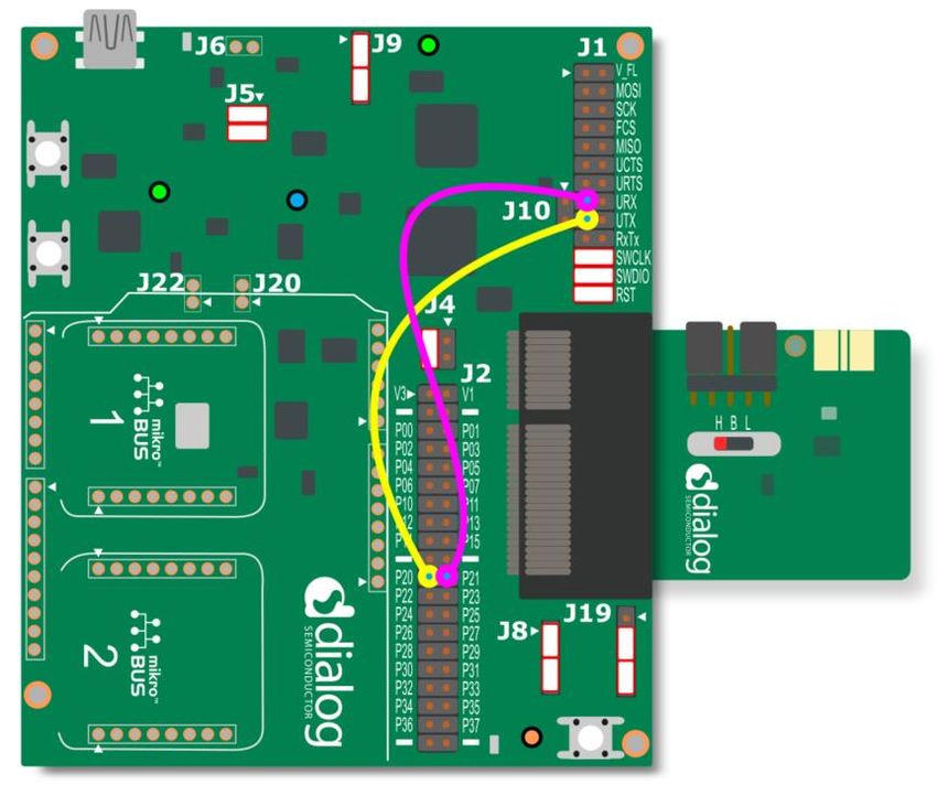
AN-B-072
DA14531 Booting from OTP and Serial Interfaces

Contents
Abstract ................................................................................................................................................ 1
Contents ............................................................................................................................................... 2
Figures .................................................................................................................................................. 3
Tables ................................................................................................................................................... 3
1    Terms and Definitions ................................................................................................................... 4
2    References ..................................................................................................................................... 4
3    Introduction.................................................................................................................................... 5
4    Booting Sequence and booting pins ........................................................................................... 5
     4.1 Timing diagram of the booting sequence .............................................................................. 6
     4.2 Reset functionality in DA14531 ............................................................................................. 7
5    Bypass mode configuration ......................................................................................................... 9
6    Booting from 1-wire UART ........................................................................................................... 9
7    Boot from 2-wire UART ............................................................................................................... 11
8    Boot from SPI Slave .................................................................................................................... 13
     8.1 Programming Flash using SWD port .................................................................................. 13
     8.2 Programming Flash using 1-wire UART ............................................................................. 16
     8.3 Programming Flash using 2-wire UART ............................................................................. 17
     8.4 Booting an encrypted image from Flash ............................................................................. 20
9    Boot from I2C ............................................................................................................................... 21
10 Boot from OTP ............................................................................................................................. 22
11 Boot from specific SPI Port ........................................................................................................ 24
12 Booting from a custom PCB ...................................................................................................... 25
13 List of supported FLASH/EEPROM memories ......................................................................... 27
14 Appendix ...................................................................................................................................... 27
   14.1 Introduction ......................................................................................................................... 27
   14.2 Booting protocols ................................................................................................................ 29
        14.2.1 Boot from SPI Bus - DA14531 Act as SPI Slave ................................................. 29
        14.2.2 Booting from UART .............................................................................................. 30
15 Conclusions ................................................................................................................................. 32
16 Revision History .......................................................................................................................... 33

Application Note                                                  Revision 1.6                                                         09-Aug-2021

CFR0014                                                                 2 of 34                                          © 2021 Dialog Semiconductor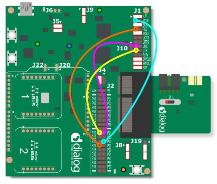
AN-B-072
DA14531 Booting from OTP and Serial Interfaces

Figures
Figure 1: DA145xx DEVKT-P PRO-Motherboard + DA14531 daughterboard ...................................... 5
Figure 2: Scan timing for booting from external serial devices ............................................................. 6
Figure 3: Step 1 to step 6 of the booting sequences zoomed in picture ............................................... 6
Figure 4: Timing diagram ....................................................................................................................... 7
Figure 5: DA14531 Reset ...................................................................................................................... 8
Figure 6: Jumper settings for Bypass mode on J4 ................................................................................ 9
Figure 7: Jumper settings for 1-wire UART ......................................................................................... 10
Figure 8: SmartSnippets™ Toolbox settings ....................................................................................... 10
Figure 9: Board Setup and Booter ....................................................................................................... 11
Figure 10: 1-wire UART booter logs .................................................................................................... 11
Figure 11: Jumper settings for 2-wire UART (P0_0 and P0_1)........................................................... 12
Figure 12: Board setup for 2-wire UART ............................................................................................. 12
Figure 13: Jumper settings for SPI Flash ............................................................................................ 14
Figure 14: JTAG selection for SPI Flash ............................................................................................. 14
Figure 15: SPI Flash pin configuration ................................................................................................ 15
Figure 16: SPI Flash programmer to connect, read and burn the hex file .......................................... 15
Figure 16: Program a hex/bin file into Flash........................................................................................ 16
Figure 18: Jumper settings 1-wire UART with SPI Flash .................................................................... 16
Figure 19: UART/SPI selection............................................................................................................ 17
Figure 20: SPI Flash pin configuration ................................................................................................ 17
Figure 21: Jumper settings 2-wire UART with SPI Flash .................................................................... 18
Figure 22: The OTP header burned with new values .......................................................................... 18
Figure 23: SYS_CTRL_REG (Debugger Bit) programming in the application level ........................... 19
Figure 24: SYS_CTRL_REG programming using OTP configuration script ....................................... 19
Figure 25: DA14531/DA14585 Booting an encrypted image from Flash ............................................ 20
Figure 25: Toolbox I2C pin configuration ............................................................................................ 21
Figure 26: Toolbox EEPROM Programmer ......................................................................................... 21
Figure 27: Toolbox OTP Programmer ................................................................................................. 22
Figure 28: OTP Boot Energy Power Profile ......................................................................................... 23
Figure 29: FTDI and DA14531 connection circuit for Reset ................................................................ 26
Figure 30: Reset line on the daughterboard with R30 resistor ............................................................ 26
Figure 31: RESET circuit on the Pro-DK Motherboard with R347 resistor ......................................... 26
Figure 32: Boot Rom sequence ........................................................................................................... 28

Tables
Table 1: Booting sequence and booting pins for silicon DA14531AE(WLCSP17) & DA14531
AE(FCGQFN24) SoC ............................................................................................................................ 5
Table 2: Boot energy - external SPI Slave .......................................................................................... 13
Table 3: Boot Energy OTP .................................................................................................................. 22
Table 4: Boot from specific SPI Port ................................................................................................... 24
Table 5: Boot Protocol - DA14531 as SPI Slave ................................................................................. 29
Table 6: SPI Master Data Communication .......................................................................................... 30
Table 7: Boot Protocol ......................................................................................................................... 31
Table 8: Boot Protocol ......................................................................................................................... 31

Application Note                                              Revision 1.6                                                     09-Aug-2021

CFR0014                                                             3 of 34                                       © 2021 Dialog Semiconductor
AN-B-072
DA14531 Booting from OTP and Serial Interfaces

1      Terms and Definitions
SoC                System on Chip
POR                Power on Reset
BLE                Bluetooth Low Energy
OTP                One-Time Programmable
HCI                Host Controller Interface
GTL                Generic Transport Layer

2      References
[1]   DA14531 Datasheet
[2]   SmartSnippets Toolbox User Manual
[3]   AN-B-075 DA14531 Hardware Guidelines
[4]   AN-B-088 Flash Selector Guide
[5]   UM-B-119 DA14585/DA14531 SW Platform Reference Manual

Application Note                          Revision 1.6                  09-Aug-2021

CFR0014                                        4 of 34        © 2021 Dialog Semiconductor
AN-B-072
DA14531 Booting from OTP and Serial Interfaces
3 Introduction
The document gives an overview of the booting options available for the DA14531 device using the
DA145xx DEVKT-P PRO-Motherboard. The boot ROM will be executed when a POR or a HW Reset
occurs or a RESET_ON_WAKEUP event happens which is a configurable feature. This document
describes the available methods to connect, boot and program the external Flash/EEPROM or the
internal OTP.
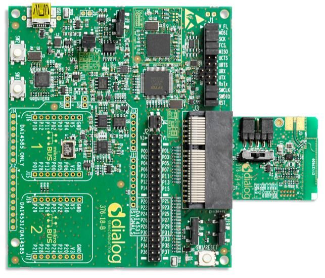
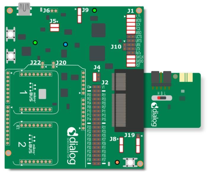
Figure 1: DA145xx DEVKT-P PRO-Motherboard + DA14531 daughterboard
4 Booting Sequence and booting pins
The booting sequence is shown in Table 1 along with the corresponding booting pins that are used.
Please refer to Booting from serial interfaces chapter to know more on the booting sequence and
booting protocols.
Table 1: Booting sequence and booting pins for silicon DA14531AE(WLCSP17) & DA14531
AE(FCGQFN24) SoC
Step 1 Step 2 Step 3 Step 4 Step 5 Step 6
Boot from Boot from Boot from 1 Boot from Boot Boot from
ext SPI 1 wire wire UART 2 wire from ext I2C
Master UART UART SPI
(2nd option)
(1st option) Slave
P0_0/RST MISO Tx MOSI
P0_1 MOSI Rx SCS
P0_2
P0_3 SCS RxTx MISO SDA
P0_4 SCK SCK SCL
P0_5 RxTx
Application Note Revision 1.6 09-Aug-2021
CFR0014 5 of 34 © 2021 Dialog Semiconductor
AN-B-072
DA14531 Booting from OTP and Serial Interfaces

Note: The booter will try to boot from the above serial interfaces in the order from Step 1 to step 6.

4.1       Timing diagram of the booting sequence
The boot ROM code execution time for booting from an external serial device is 17.3ms. At the end of
the scanning sequence the device will halt with the JTAG enabled (if there is no disabling from the
configuration script). Figure 2 displays the power-up sequence of the DA14531 and pins P0_0 to P0_5,
which are involved in the 6 steps as explained in booting sequence Table 1.

                  Figure 2: Scan timing for booting from external serial devices

Figure 3 gives the overview of the booting steps from step 1 to step 6.

              Figure 3: Step 1 to step 6 of the booting sequences zoomed in picture

Figure 4 shows the scan timing from the external devices when there are no external devices
available on any of the possible interfaces to boot from. The approximate time to boot from each
peripheral is also noted.

Application Note                            Revision 1.6                                   09-Aug-2021

CFR0014                                         6 of 34                          © 2021 Dialog Semiconductor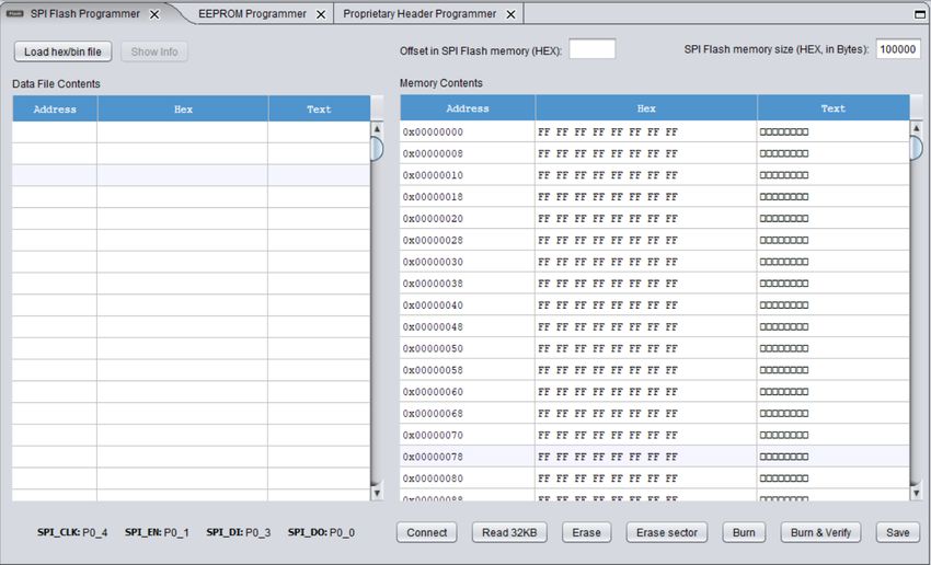
AN-B-072
DA14531 Booting from OTP and Serial Interfaces

                                      Figure 4: Timing diagram

As seen in the above Timing diagram, step 1 could not be captured in the zoomed in figure. Please
refer to Figure 3 for the capture. The booting of DA14531 is incredibly fast and the above timing
diagram can help the developer to select the booting most suitable for their application.

4.2       Reset functionality in DA14531
The reset functionality POR (Power-On Reset) or HW reset (hardware) on P0_0 is multiplexed with
SPI Slave MOSI and UART Tx. It is disabled when the P0_0 is used as a peripheral pin for 2-wire
UART or SPI. Please refer to Figure 2 to see the behavior P0_0 during booting.
After the booting, the reset functionality on the P0_0 is restored.
To configure the functionality of triggering a POR by a GPIO pin, follow the steps below:
   1. Select a GPIO to be set as the POR source by programming
      POR_PIN_REG[POR_PIN_SELECT].
   2. Set up the input polarity of the GPIO that causes POR by programming
      POR_PIN_REG[POR_PIN_POLARITY].
   3. Configure the time for the POR to happen by programming POR_TIMER_REG[POR_TIME].
      The default time is around three seconds.

To be able to enable POR on a GPIO from the application software, the SDK has a function that can
be used for this.
GPIO_EnablePorPin(GPIO_PORT port, GPIO_PIN pin, GPIO_POR_PIN_POLARITY polarity,
uint8_t por_time);
port       - GPIO port
pin        - GPIO pin
polarity - GPIO port pin polarity. Active low = 0, Active high = 1.
por_time - Time for the Power-On Reset to happen. The time is calculated based on the following
            equation: Time = por_time x 4096 x RC32 clock period
Example: To configure GPIO PORT 0 and PIN 7 (P0_7) as POR with a default POR time as 3
seconds and setting the polarity as active high,
GPIO_EnablePorPin(GPIO_PORT_0, GPIO_PIN_7, 1 , 0x18);

Application Note                             Revision 1.6                              09-Aug-2021

CFR0014                                          7 of 34                     © 2021 Dialog Semiconductor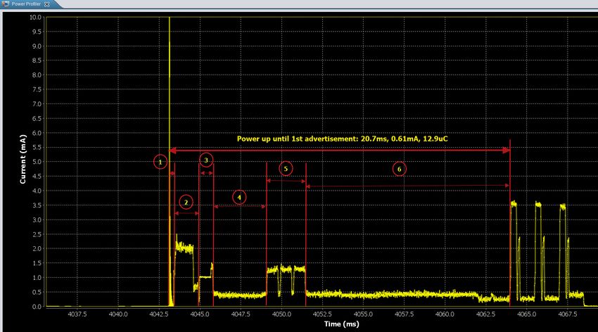
AN-B-072
DA14531 Booting from OTP and Serial Interfaces

Calling this function, say after the system_init() will enable P0_7 to be a POR GPIO.

int main(void)
{
    sleep_mode_t sleep_mode;
    // initialize retention mode
    init_retention_mode();
    //global initialise
    system_init();
    GPIO_EnablePorPin(GPIO_PORT_0, GPIO_PIN_7, 1 , 0x18);
    .
    .
}

To trigger a POR via P0_7 at application code run time, connect a with a fly wire from P0_7 to J2[V3]
of the motherboard for more than 3seconds. Then the device will reset with POR event.

                                     Figure 5: DA14531 Reset

Please be aware if a GPIO is used as a POR source, the dynamic current of the system increases due
to the dynamic current consumed by the RC32k oscillator. This increase is estimated to be from 100
nA to 120 nA and it is also present during sleep time period. POR from the RST pad does not add this
dynamic current consumption.
Please note the POR functionality is not supported in the hibernation mode.
For more details on the reset pin mapping on DA14531 refer the Chapter 5 of the datasheet.

Application Note                          Revision 1.6                                  09-Aug-2021

CFR0014                                       8 of 34                         © 2021 Dialog Semiconductor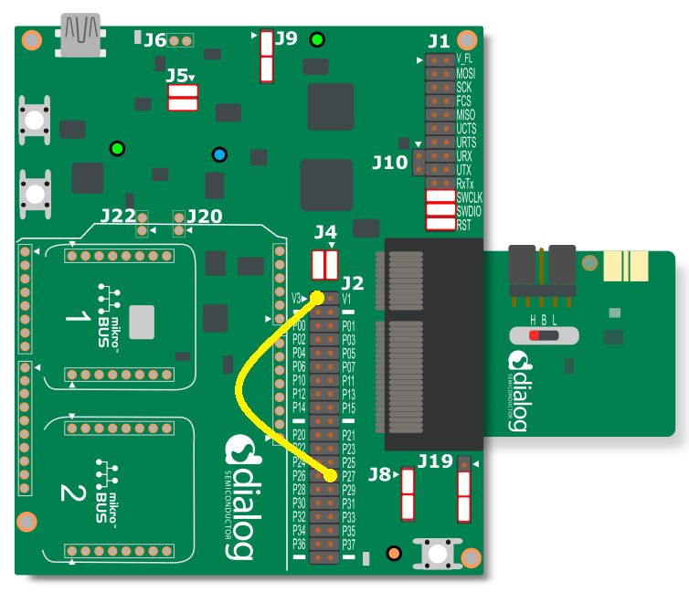
AN-B-072
DA14531 Booting from OTP and Serial Interfaces

5     Bypass mode configuration
When the DA14531 is configured to run in Buck or Boost mode, the SDK auto-configures the mode
depending on the power supply scheme (jumper settings on J4 on the motherboard). However, to run
in Bypass mode, the appropriate flag needs to be set in the SDK in the da1458x_config_basic.h file
of the project. This will configure the device to Bypass mode.
#define CFG_POWER_MODE_BYPASS

The jumper settings on J4 jumper for Buck or Boost mode is described in Chapter 6 How to
Configure Power of DA14531 DK PRO of UM-B-114
The jumper settings that goes in the motherboard on J4 for the Bypass mode is as shown in Figure 6

                       Figure 6: Jumper settings for Bypass mode on J4

6     Booting from 1-wire UART
The bootloader of the DA14531 supports 1-wire UART interface on pin P0_5 or P0_3 which is step 2
or step 3 of the booting sequence. To boot from P0_3, connect the FTDI RX and TX via a 1K resistor
and connect the RX side of FTDI to the P0_3 pin. Please note the 1K resistor exists in the mother
board, when using it there is no need do that.
The jumper settings to use the 1-wire UART are as shown in the Figure 7. They are marked as white
box with red outline. The jumpers are set to enable the 1-wire UART functionality along with SWD but
not the Flash. Using flash and 1-wire UART is described in the coming sections.

Application Note                          Revision 1.6                                 09-Aug-2021

CFR0014                                       9 of 34                        © 2021 Dialog Semiconductor
AN-B-072
DA14531 Booting from OTP and Serial Interfaces

                          Figure 7: Jumper settings for 1-wire UART

Booting on the 1 wire UART using the SmartSnippets™ Toolbox requires following settings,
● Select the following SmartSnippets™ settings as shown in Figure 8 to boot from UART

                          Figure 8: SmartSnippets™ Toolbox settings

● Select P0_5, P0_5, 115200 Bd in the Board Setup and in the boot ROM browse through the
   binary you want to download to SysRAM as shown in the figure below,

Application Note                         Revision 1.6                                09-Aug-2021

CFR0014                                     10 of 34                       © 2021 Dialog Semiconductor
AN-B-072
DA14531 Booting from OTP and Serial Interfaces
Figure 9: Board Setup and Booter
● Check the logs to confirm the firmware download as shown in Figure 10 and now the device will
boot from 1-wire UART.
Figure 10: 1-wire UART booter logs
7 Boot from 2-wire UART
The bootloader of the DA14531 supports 2-Wire UART interface on pin P0_0 and P0_1. The hardware
and software setup are like 1-wire UART except for the jumper settings and board setup as shown in
Figure 11 and Figure 12.
Application Note Revision 1.6 09-Aug-2021
CFR0014 11 of 34 © 2021 Dialog SemiconductorAN-B-072
DA14531 Booting from OTP and Serial Interfaces
Figure 11: Jumper settings for 2-wire UART (P0_0 and P0_1)
For the 2-wire UART, the board setup is as shown below,
Figure 12: Board setup for 2-wire UART
The jumper settings on the motherboard from J1 to J2 header is as shown in Figure 9. The UTX (of
the FTDI chip) is connected using a jumper cable to J2-P20 (P0_0/UART-Tx of the DA14531) and URX
(of the FTDI chip) is connected to J2-P21 (P0_1/UART-Rx of the DA14531).
Using the Booter from the SmartSnippets™Toolbox, download the firmware and the DA14531 will boot
from the 2-wire UART as per the step 4 of the boot sequence.
Application Note Revision 1.6 09-Aug-2021
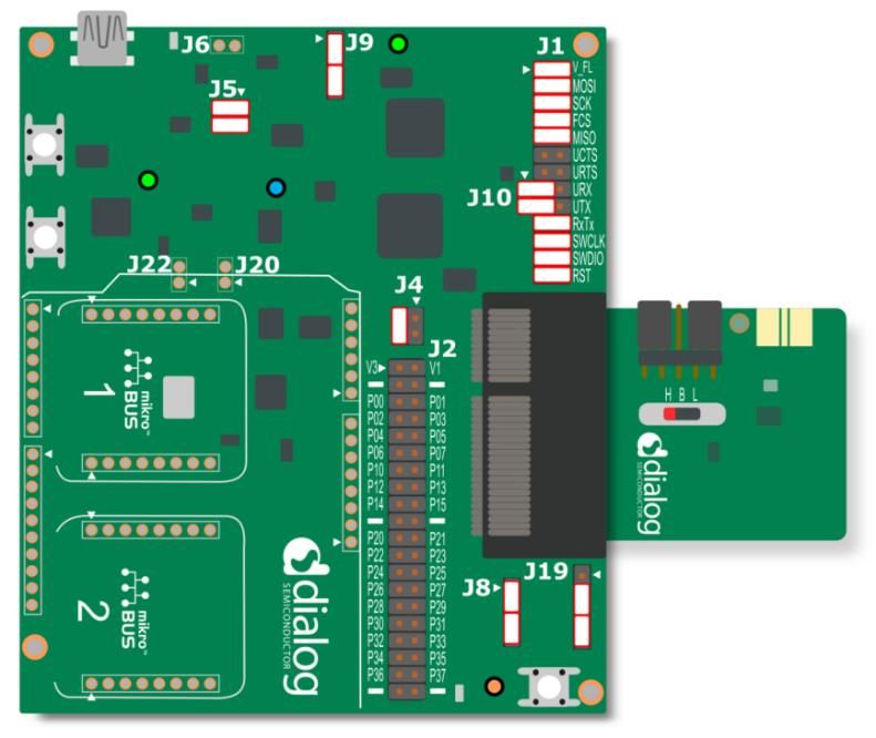
CFR0014 12 of 34 © 2021 Dialog SemiconductorAN-B-072 DA14531 Booting from OTP and Serial Interfaces 8 Boot from SPI Slave Booting from external SPI Slave is the 5th step in the booting sequence for the DA14531 and the sequence of events that takes place after the power up is described in the table below following with the power profile. The following table is with respect to the BUCK mode wherein 13.1kB (BLE Barebone) application is copied from the external Slave SPI with speed of 2MHz speed. Table 2: Boot energy - external SPI Slave Interval Time (ms) Average current (mA) Charge (uC) Power Up and 1.05 6.94 7.5 HW FSM OTP Enabled & XTAL Settling 4.53 1.84 17.1 Booter steps 1-4 9.63 1.13 10.9 Booting from the 3.22 SPI slave 57.8 189.0 Total 73.01 3.06 255.2 8.1 Programming Flash using SWD port Use the jumper settings on the motherboard as shown in the picture below. The onboard 2-Mbit SPI data flash (MX25R2035) memory is connected over SPI to the DA14531 can be accessed over the SWD port. The description below will explain how to program the firmware into the Flash memory. The necessary motherboard jumper settings are shown in Figure 13. Application Note Revision 1.6 09-Aug-2021 CFR0014 13 of 34 © 2021 Dialog Semiconductor
AN-B-072
DA14531 Booting from OTP and Serial Interfaces

                            Figure 13: Jumper settings for SPI Flash

In the SmartSnippets™ toolbox, please select the following as shown in Figure 14 for JTAG
interface,

                             Figure 14: JTAG selection for SPI Flash

After you click on Open, do the SPI Pin configuration as shown in the Figure 15 below,
MOSI (SPI_DO) - P0_0
CS (SPI_EN) - P0_1
MISO (SPI_DI) - P0_3
CLK (SPI_CLK)- P0_4

Application Note                          Revision 1.6                                   09-Aug-2021

CFR0014                                       14 of 34                        © 2021 Dialog Semiconductor
AN-B-072
DA14531 Booting from OTP and Serial Interfaces
Figure 15: SPI Flash pin configuration
In the Layout tab, select SPI Flash/ EEPROM and you will SPI Flash Programmer tab opens as
shown in Figure 16 below.
Figure 16: SPI Flash programmer to connect, read and burn the hex file
Using the Load hex/bin file button, browse through the location for the hex or binary file that you
want to download to the device as shown below. Select Bootable as shown, to make the device
bootable. Click on Next and then Finish.
Application Note Revision 1.6 09-Aug-2021
CFR0014 15 of 34 © 2021 Dialog SemiconductorAN-B-072
DA14531 Booting from OTP and Serial Interfaces
Figure 17: Program a hex/bin file into Flash
Click on Connect and if it prompts to press the hardware Reset button, press the reset button on the
motherboard. Please look at the SmartSnippets™ Toolbox log to make sure the default
jtag_programmer is loaded in the SysRAM.
Once connected, you can erase/read or Flash the program.
Click Burn to program the flash using the SPI slave interface. Check the SmartSnippets™ Toolbox log
file to make sure the firmware is successfully programmed in the flash memory. Press the hardware
RESET button on the motherboard and now the device will boot from the SPI flash.
8.2 Programming Flash using 1-wire UART
The Flash memory connected over SPI to the DA14531 can be accessed over the 1-wire UART. The
description below will explain how to program the firmware into the Flash memory. To boot from SPI
Slave using the 1-wire UART, the jumper settings and the board setup are shown in the Figure 18.
Figure 18: Jumper settings 1-wire UART with SPI Flash
Application Note Revision 1.6 09-Aug-2021
CFR0014 16 of 34 © 2021 Dialog SemiconductorAN-B-072
DA14531 Booting from OTP and Serial Interfaces
Figure 19: UART/SPI selection
Once you have these configurations, the following steps to connect/ read/ write / erase are like in
Chapter 8.1
8.3 Programming Flash using 2-wire UART
The Flash memory connected over SPI to the DA14531 can be accessed over the 2-wire UART. The
description below will explain how to program the firmware into the Flash memory. To boot from SPI
Slave using the 2-wire UART, the jumper settings and the board setup are shown in Figure 20.
To boot from SPI Slave using the 2-wire UART needs a modification in the pin configuration due to the
reason that the P0_0 is multiplexed between DA14531-UART Tx and SPI slave MOSI. Due to this
reason we modify the pin configuration in the following way as shown below.
Figure 20: SPI Flash pin configuration
Application Note Revision 1.6 09-Aug-2021
CFR0014 17 of 34 © 2021 Dialog SemiconductorAN-B-072
DA14531 Booting from OTP and Serial Interfaces
MOSI (SPI_DO) - P0_5
CS (SPI_EN) - P0_6
MISO (SPI_DI) - P0_3
CLK (SPI_CLK)- P0_4
The jumper setting would be as shown in Figure 21.
Figure 21: Jumper settings 2-wire UART with SPI Flash
The DA14531 bootloader is capable of booting from a specific booting path (new SPI pin
assignment). We simply need to use the configuration properly by applying it in the OTP header
fields. An application can determine by using the OTP header fields which SPI pins the boot ROM
should use for booting from an external non-volatile memory.
The OTP header breakdown on the 0x7F87FC8 and 0x7F87FCC addresses is
presented in Table 4.
On address 0x7F87FC8 the application should program: 0x00FFABAA
On address 0x7F87FCC the application should program: 0x03050604
Figure 22: The OTP header burned with new values
Application Note Revision 1.6 09-Aug-2021
CFR0014 18 of 34 © 2021 Dialog SemiconductorAN-B-072
DA14531 Booting from OTP and Serial Interfaces
Note: Section 11 Boot from specific SPI Port provides more details about Booting from Specific SPI
port.
Note: The SWD interface is disabled when OTP is programmed on DA14531. It is possible to re-
enable SWD in your application code via the configuration script. You need to program 0x1A1 to the
SYS_CTRL_REG (P0_2/P0_10).
Note: If the Firmware burned in the OTP has the debugger enabled, then the SWD interface will be
enabled from the application itself without explicitly burned the configuration script.
Figure 23: SYS_CTRL_REG (Debugger Bit) programming in the application level
Note: For application code mentioning the DEBUGGER_ENABLE bits in SYS_CTRL_REG as just
writing 0x1A1 to this register in application code can result in unexpected behaviour, especially as
this will remap OTP at 0x00000000 when a reset is triggered.
For OTP programming procedures refer to the section 14 in the SmartSnippets Toolbox User
Manual.
Once you have these configurations, the following steps to connect/ read/ write / erase are like in
Chapter 8 above.
Figure 24: SYS_CTRL_REG programming using OTP configuration script
Application Note Revision 1.6 09-Aug-2021
CFR0014 19 of 34 © 2021 Dialog SemiconductorAN-B-072
DA14531 Booting from OTP and Serial Interfaces
8.4 Booting an encrypted image from Flash
The DA14531/DA14585 can boot from external flash or MCU by copying the content to SRAM. The
SDK6 supports booting from an encrypted image, in fact during the boot time the CPU will decrypt
the image using the AES128 algorithm and store it in SRAM, the encryption keys are stored in OTP
and the serial wire debug port must be disabled to prevent hackers to read out the encryption keys. If
an encrypted image is burned in the SPI flash (or other resource) the booting can be done only if the
secondary bootloader is used. The basic bootloader which runs from the ROM can’t do the
decryption of an encrypted image. A secondary bootloader is required to do the decryption. For the
secondary bootloader creation, you can refer to the section 6.2 in [5]. In the bootloader.h under the
secondary bootloader project in this location: 6.0.14.1114\utilities\secondary_bootloader
The SDK is defining this flag:
/************** Encrypted Image Support section**************/
#define AES_ENCRYPTED_IMAGE_SUPPORTED 1
Note: The SUOTA of encrypted images is supported and the tools to encrypt the image are provided.
Figure 25: DA14531/DA14585 Booting an encrypted image from Flash
Application Note Revision 1.6 09-Aug-2021
CFR0014 20 of 34 © 2021 Dialog SemiconductorAN-B-072
DA14531 Booting from OTP and Serial Interfaces
9 Boot from I2C
Using the EEPROM Programmer in SmartSnippets™ Toolbox you can download the image to the
EEPROM memory and boot from the EEPROM. The SDA and SCL lines to be selected in the board
setup are P0_3 and P0_4 respectively.
Figure 26: Toolbox I2C pin configuration
The breakout for the 531 on the Motherboard would be P2_3 and P2_4, so connect the SDA and SCL
to P2_3 and P2_4 using jumper cables.
Now click on “Connect” and once connected select the firmware to download to the EEPROM memory.
Figure 27: Toolbox EEPROM Programmer
Application Note Revision 1.6 09-Aug-2021
CFR0014 21 of 34 © 2021 Dialog SemiconductorAN-B-072
DA14531 Booting from OTP and Serial Interfaces
10 Boot from OTP
The OTP (One-Time Programmable) Programmer tool in the SmartSnippets™ Toolbox is used for
burning the OTP Memory and OTP Header. Once this is programmed, it cannot be erased.
Set the right application flags to be able to boot from the OTP. The Application Flag 1 and Application
Flag 2 are set to “YES” as shown in Figure 28. The OTP DMA length can be set as hexadecimal value
equal to the code binary size divided by 4. To do this, open the .bin file in any hex editor which will give
the length of the code. Dividing this by 4 will give the OTP DMA length value to be entered (in
Hexadecimal). This field can also be left blank, however, entering this value results in slightly quicker
execution of code from the OTP.
Once these values of the header are set, connect and burn the OTP header.
Note: The application flag 1 and application flag 2 should be set to value "Yes" as shown in Figure
28.
Figure 28: Toolbox OTP Programmer
On the OTP Image tab, select the file to download and burn to OTP. After burning the header and the
image, the device will be able to boot from OTP and bypass the ROM boot sequence as described in
Chapter 4.
The boot energy analysis in BUCK configuration can be found in Table 3 and the power profile from
power-up until the first BLE advertisement is shown in .
Table 3: Boot Energy OTP
Sl.No. Events Time (ms) Average current (mA) Charge (uC)
Power up, HW FSM
1 until OTP CS read 0.35 1.82 0.64
OTP CS reading
(1.24ms), XTAL
settling until RF
2 calibration 1.49 1.68 2.51
3 OTP mirroring 0.87 1.03 0.9
OTP mirroring to RF
4 calibration 3.2 0.38 1.25
5 RF calibration 2.4 1.16 2.8
Application Note Revision 1.6 09-Aug-2021
CFR0014 22 of 34 © 2021 Dialog SemiconductorAN-B-072
DA14531 Booting from OTP and Serial Interfaces
SW initialization,
BLE initialization,
6 application start 12.4 0.38 4.81
Total 20.71 0.61 12.91
Figure 29: OTP Boot Energy Power Profile
For more details, please check the SmartSnippetsTM Toolbox User Manual.
Application Note Revision 1.6 09-Aug-2021
CFR0014 23 of 34 © 2021 Dialog SemiconductorAN-B-072
DA14531 Booting from OTP and Serial Interfaces
11 Boot from specific SPI Port
In Development mode, the "Boot from Specific" flag will be evaluated. If the flag is programmed, new
pin locations for booting from an external SPI slave to make DA14531 an SPI Master will be set. The
"Boot from Specific" flag can be addresses when for instance to boot FW from external SPI Flash
with different SPI Pins assignment. The details of the configuration are presented below. If this path
is entered, the system will always try to boot from UART so that the SPI Flash can be updated if
needed. Any of the three UART configurations specified in Table 4 can be selected by writing bits
[31:24] at the "Boot specific config" field in the OTP header. If booting from SPI Flash fails, the Booter
will jump back to the normal scan sequence of the peripheral devices.
The advantages are, the booter will skip other scan sequence of peripheral devices, thereby reducing
the boot time from SPI slave. From Table 1, the boot step 1-4 time will thereby be negligible. Also,
the SPI Clock speed can be increased to reduce the time to copy code from Flash to SysRAM.
Figure 22 is an example of the values set in the OTP header for the boot specific mode.
The table below is taken from the datasheet, section 4.4 OTP header.
Table 4: Boot from specific SPI Port
Address Name Description
0x07F87FC8 Boot specific config Boot specific configuration:
● Bits[7:0] : ○ 0xAA = Boot from SPI port at a specific location
○ 0xFF = Normal sequence
● Bits[15:8] = Wake up Command opcode
● Bits[23:16] = SPI_DIV
● Bits[31:24]:
○ 0x00 = Two-wire UART (P0_0/P0_1)
○ 0x01 = One-wire UART (P0_3)
○ 0x02 = One-wire UART (P0_5)
○ Default (all other values) = Two-wire UART (P0_0/P0_1)
0x07F87FCC Boot specific port Boot specific port mapping:
mapping Bits[7:4] = SPI_CLK, Port number
Bits[3:0] = SPI_CLK, Pin number
Bits[15:12] = SPI_EN, Port number
Bits[11:8] = SPI_EN, Pin number
Bits[23:20] = SPI_DO, Port number
Bits[19:16] = SPI_DO, Pin number
Bits[31:28] = SPI_DI, Port number
Bits[27:24] = SPI_DI, Pin number
Application Note Revision 1.6 09-Aug-2021
CFR0014 24 of 34 © 2021 Dialog SemiconductorAN-B-072
DA14531 Booting from OTP and Serial Interfaces
• In address 0x07F87FC8 which is boot specific config,
Bits[31:24]: 02 (1-wire UART P0_5)
Bits[23:16]: 7F (SPI_DIV, clock speed, 7F gives the maximum clock speed for SPI. 8MHz
can be achieved using the DA14531 module)
Bits[15:8]: AB (wake up command opcode that flash memory responds to)
Bites[7:0] : AA (0xAA implies boot from SPI Port at a specific location)
• In address 0x07F87FCC which is boot specific port mapping,
Bits[31:28] = SPI_DI, Port number = 0
Bits[27:24] = SPI_DI, Pin number = 3
Bits[23:20] = SPI_DO, Port number = 0
Bits[19:16] = SPI_DO, Pin number = 0
Bits[15:12] = SPI_EN, Port number = 0
Bits[11:8] = SPI_EN, Pin number = 1
Bits[7:4] = SPI_CLK, Port number = 0
Bits[3:0] = SPI_CLK, Pin number = 4
12 Booting from a custom PCB
When using a custom PCB to boot from 2-wire UART, it is advised to take care of the RST/P0_0 pin
such that it doesn’t continuously reset as the default setting after the boot sequence is finished is RST.
The explanation related to this is given below.
Since the idle state of the UART lines are default high, FTDI devices and microcontrollers tend to have
a pull up resistor on their RX line in order to avoid continuous break. Since the P0_0 is used as a TX
while booting and also as a HW reset, connecting an external device might continuously reset the
DA14531 due to the external pull up.
As you can see in Table 1, when booting from 2-wire UART (Step4), the Tx is mapped to P0_0 which
is also used as Reset pin. The device starting its boot sequence will detect UART on P0_0/P0_1. After
the boot sequence has finished the P0_0 will automatically be restored to reset mode. If a connected
external microcontroller or FTDI USB to UART bridge pulls this port high, it will trigger a continuous
reset.
A valid solution would be to use a stronger R pull-down resistor connected to P0_0 overriding the effect
of the receiver’s pull up, as shown in Figure 30. The value of R depends on the pull up on the receiver’s
side. This solution is acceptable if there is no constant voltage from an external device on P0_0 to leak
through the strong pull down.
In case that the application requires constant connection on the P0_0/P0_1 due to external interface
the user must make sure that during the booting process of the DA14531 the external controller will
not have its RX pin in high state since this would cause the DA14531 to reset. . If the external processor
can handle the fact that its RX line will be low thus getting continuous break conditions, then the
external pull down can be omitted.
The above configuration won't allow to reset the board from the external device (since using the P0_0
as a TX one should have the reset disabled), in that case either enable the reset again via a command
from the external processor or set a GPIO pin to act as a POR source. An alternative solution would
be to burn a secondary booter in the OTP and boot from different pins and keep the P0_0 as a reset.
On Dialog Pro-DK Motherboard this is solved by populating the resistor R30 resistor (1k) in the
daughterboard as shown in Figure 31 and connecting the reset circuit of the motherboard as shown in
Figure 32 with the R347 resistor (10k). This creates a strong pull-down. The figures below indicate part
of the reset schematics.
Application Note Revision 1.6 09-Aug-2021
CFR0014 25 of 34 © 2021 Dialog SemiconductorAN-B-072
DA14531 Booting from OTP and Serial Interfaces
Figure 30: FTDI and DA14531 connection circuit for Reset
Figure 31: Reset line on the daughterboard with R30 resistor
Figure 32: RESET circuit on the Pro-DK Motherboard with R347 resistor
Application Note Revision 1.6 09-Aug-2021
CFR0014 26 of 34 © 2021 Dialog SemiconductorAN-B-072 DA14531 Booting from OTP and Serial Interfaces 13 List of supported FLASH/EEPROM memories The memories listed in [4] are currently supported by DIALOG. These memories support the standard Serial Peripheral Interface (SPI) and I2C and operate using the 3.3 V power supply. Note: This list is not extensive and other devices compliant to the requirement spec will work as well. Note: The AT25XE041D flash is a part of the Adesto's FusionHD family the new generation of Flash from Adesto Technologies/Dialog. This family has a unique characteristic that can go to 7nA in ultra- deep power down mode (UDPD). However, it needs a secondary bootloader to work correctly with the DA14531, the reason is when the AT25XE041D goes into the UDPD mode it has a quit high time to wake up, around 260 µs which doesn’t cooperate with our boot ROM. Note: To support XE021A or XE041B, it is not necessary to modify the SPI driver software code like the AT25XE041D part number. This is an application development choice to select the proper flash part number based on either fast application prototyping or reducing power consumption of the overall system. 14 Appendix 14.1 Introduction The DA14531 can boot from external serial devices when the OTP memory is not programmed. This is to enable the development of application code. At power-up the system enters Development Mode, where the boot code decides which interface to boot from. This section describes the boot sequence for all supported serial interfaces and provides the developer with the necessary information to realize the protocol required to establish communication between an external device and the DA14531. The DA14531 operates in two modes: Normal mode and Development mode. The decision which mode the chip enters after power-up, is taken by the boot code that resides in the ROM. A complete flow chart of the boot code is illustrated below Application Note Revision 1.6 09-Aug-2021 CFR0014 27 of 34 © 2021 Dialog Semiconductor
AN-B-072
DA14531 Booting from OTP and Serial Interfaces

                                   Figure 33: Boot Rom sequence

The boot ROM code reads the Application Programmed flags from the OTP header to identify
whether the chip is in Development mode or Normal mode.
When in Development mode, the boot ROM code initializes all serial peripheral devices from which
the DA14531 might download code. The options are:
● UART
● SPI (both master and slave)
● I2C (only master)

The boot ROM code searches for a valid response on various combinations of I/O’s one after the
other. There is also the option that the user can define desired I/O’s with the use of a specific OTP
field for the SPI interface.

Application Note                            Revision 1.6                                   09-Aug-2021

CFR0014                                        28 of 34                          © 2021 Dialog Semiconductor
AN-B-072
DA14531 Booting from OTP and Serial Interfaces
The boot pins and serial peripherals search sequence are presented in the Table 1
14.2 Booting protocols
14.2.1 Boot from SPI Bus - DA14531 Act as SPI Slave
The boot ROM code initially configures the DA14531 SPI controller with the following parameters:
● 8 bit mode
● Slave role
● Mode 0: SPI clock is initially expected to be low and SPI phase is zero.
The protocol required to establish a successful communication and to download the SW into the
RAM is given in
Table 5: Boot Protocol - DA14531 as SPI Slave
Byte Nr DA14531 MOSI DA14531 MISO
0 Preamble: 0x70
1 Preamble: 0x50
2 Empty: 0x00
3 Preamble ACK: 0x02
Length LS byte Preamble NACK:0x20
4 Length MS byte
5 CRC byte
6 Length ACK:0x02
Mode byte Length NACK:0x20
7 Empty: 0x00
8 Code/Mode ACK:0x02
Data bytes Code/Mode NACK:0x20
The external SPI master device starts by sending the Preamble bytes (0x70 and 0x50) followed by a
zero byte. The DA14531 confirms the reception of the Preamble with 0x02 (Acknowledged) or 0x20
(Not Acknowledged) in case something went wrong. Bytes 3 and 4 define the length of the payload to
follow. The least significant byte is sent first. The length is a number that represents the amount of data
in 32-bit words.
Next, the SPI master must send the calculated CRC of the payload. The CRC is calculated by XORing
every successive byte with the previous value. Initial CRC value is 0xFF.
Byte 6 defines the mode of operation directed by the SPI master (8, 16 or 32-bit modes) while the
DA14531 SPI slave answers with ACK/NACK regarding the reception of the length bytes.
The mode is encoded as follows:
Application Note Revision 1.6 09-Aug-2021
CFR0014 29 of 34 © 2021 Dialog SemiconductorAN-B-072
DA14531 Booting from OTP and Serial Interfaces
0x00 = 8-bit mode
0x01 = 16-bit mode
0x02 = 32-bit mode
0x03 = Reserved
Byte 8 is the last control byte, where DA14531 replies with ACK/NACK with regards to the reception
of the CRC and the mode, while the external SPI master starts to send the first byte of the payload
(least significant byte of the first word).
The data section is presented in and takes into consideration the instructed mode. The stream of
data is followed by 2 extra empty slots to provide the required time to the DA14531 SPI controller to
compute the CRC and answer with ACK/NACK.
Upon completion of the SPI master process, all related pads are set to input and pulled down.
Table 6: SPI Master Data Communication
Slot Nr. MOSI (8-bit MOSI (16-bit mode) MOSI (32-bit mode) MISO
mode)
0 byte 1, byte 0 byte 3, byte 2, byte 1,
byte 0
byte 0
1 byte 3, byte 2 byte 7, byte 6, byte 5,
byte 1
byte 4
…
4*Len-1 or 16-bit word (2*Len-1) 32-bit word (Len-1)
byte (4*Len-
2*Len-1 or
1)
Len-1
All 0x00 All 0x00 All 0x00 All 0x00
ACK: 0x02
All 0x00 All 0x00 All 0x00 NACK: 0x20
14.2.2 Booting from UART
The boot ROM code initially configures the DA14531 UART controller with the following parameters:
● Bits: 8
● No parity
● 1 stop bit
● Baud rate: fixed at 115.2 Kbps for DA14531
The protocol required to establish successful communication and to download the SW image into the
RAM is shown in the next tables depending on the chip:
Application Note Revision 1.6 09-Aug-2021
CFR0014 30 of 34 © 2021 Dialog SemiconductorAN-B-072
DA14531 Booting from OTP and Serial Interfaces
Table 7: Boot Protocol
Byte Nr DA14531 Tx DA14531 Rx
0 STX = 0x02
1 SOH = 0x01
2 LEN_LSB byte
3 LEN_MSB byte
4 ACK = 0x06 or NACK = 0x15
5 to N SW code bytes
N+1 CRC
N+2 ACK = 0x06
The protocol starts with the DA14531 UART TX pin that transmits 0x02 (Start TX - STX). The external
device is expected to answer with a 0x01 (Start of Header - SOH) byte followed by 2 more bytes
(LEN_LSB, LEN_MSB), which define the length of the code to be downloaded (first byte is the least
significant, second the most significant). The DA14531 answers with 0x06 (ACK) if the 3 bytes have
been received and SOH has been identified, or answers with 0x15 (NACK) if anything went wrong.
At this point the connection has been successfully established and the SW code will start to be
downloaded. The next N bytes are received and put into the RAM and starts at address 0x07FC0000
as shown in Table 8.
Table 8: Boot Protocol
Address Byte 3 (MSB) Byte 2 Byte 1 Byte 0
0x07FC0000 Code byte 3 Code byte 2 Code byte 1 Code byte 0
0x07FC0004 … Code byte 5 Code byte 5
…
Application Note Revision 1.6 09-Aug-2021
CFR0014 31 of 34 © 2021 Dialog SemiconductorAN-B-072 DA14531 Booting from OTP and Serial Interfaces 15 Conclusions This document described the booting options available for the DA14531. Using this information, the user can select the best booting options for the end application. Application Note Revision 1.6 09-Aug-2021 CFR0014 32 of 34 © 2021 Dialog Semiconductor
AN-B-072
DA14531 Booting from OTP and Serial Interfaces

16 Revision History
 Revision     Date         Description
 1.0          04-11-2019   Initial version
 1.1          11-02-2020   Added section Booting from custom PCB
 1.2          12-03-2020   Added section 5 and updated few sections
 1.3          10-05-2020   Added list of supported flash/eeprom memories section
 1.4          30-06-2020   Document title update, Boot from OTP numbers update, Boot specific
                           section 11 added, Booting protocols added
 1.5          04-01-2021   Sections 8.3 and 13 updated. Section 8.4 added
 1.6          09-08-2021   Fix typo in Figure 22

Application Note                  Revision 1.6                                     09-Aug-2021

CFR0014                                33 of 34                        © 2021 Dialog Semiconductor
AN-B-072
DA14531 Booting from OTP and Serial Interfaces
Status Definitions
Status Definition
DRAFT The content of this document is under review and subject to formal approval, which may result in modifications or
additions.
APPROVED The content of this document has been approved for publication.
or unmarked
Disclaimer
Information in this document is believed to be accurate and reliable. However, Dialog Semiconductor does not give any representations or
warranties, expressed or implied, as to the accuracy or completeness of such information. Dialog Semiconductor furthermore takes no
responsibility whatsoever for the content in this document if provided by any information source outside of Dialog Semiconductor.
Dialog Semiconductor reserves the right to change without notice the information published in this document, including without limitation the
specification and the design of the related semiconductor products, software and applications.
Applications, software, and semiconductor products described in this document are for illustrative purposes only. Dialog Semiconductor makes
no representation or warranty that such applications, software and semiconductor products will be suitable for the specified use without further
testing or modification. Unless otherwise agreed in writing, such testing or modification is the sole responsibility of the customer and Dialog
Semiconductor excludes all liability in this respect.
Customer notes that nothing in this document may be construed as a license for customer to use the Dialog Semiconductor products, software
and applications referred to in this document. Such license must be separately sought by customer with Dialog Semiconductor.
All use of Dialog Semiconductor products, software and applications referred to in this document are subject to Dialog Semiconductor’s Standard
Terms and Conditions of Sale, available on the company website (www.dialog-semiconductor.com) unless otherwise stated.
Dialog and the Dialog logo are trademarks of Dialog Semiconductor plc or its subsidiaries. All other product or service names are the property of
their respective owners.
© 2021 Dialog Semiconductor. All rights reserved.
Contacting Dialog Semiconductor
United Kingdom (Headquarters) North America Hong Kong China (Shenzhen)
Dialog Semiconductor (UK) LTD Dialog Semiconductor Inc. Dialog Semiconductor Hong Kong Dialog Semiconductor China
Phone: +44 1793 757700 Phone: +1 408 845 8500 Phone: +852 2607 4271 Phone: +86 755 2981 3669
Germany Japan Korea China (Shanghai)
Dialog Semiconductor GmbH Dialog Semiconductor K. K. Dialog Semiconductor Korea Dialog Semiconductor China
Phone: +49 7021 805-0 Phone: +81 3 5769 5100 Phone: +82 2 3469 8200 Phone: +86 21 5424 9058
The Netherlands Taiwan
Dialog Semiconductor B.V. Dialog Semiconductor Taiwan
Phone: +31 73 640 8822 Phone: +886 281 786 222
Email: Web site:
enquiry@diasemi.com www.dialog-semiconductor.com
Application Note Revision 1.6 09-Aug-2021
CFR0014 34 of 34 © 2021 Dialog SemiconductorYou can also read